This thread has been locked.

If you have a related question, please click the "Ask a related question" button in the top right corner. The newly created question will be automatically linked to this question.

UCC27211: Make high side switch of synchronous buck converter bidirectional (back to back mosfet)

Part Number: UCC27211
Other Parts Discussed in Thread: TPS2411

Current application:

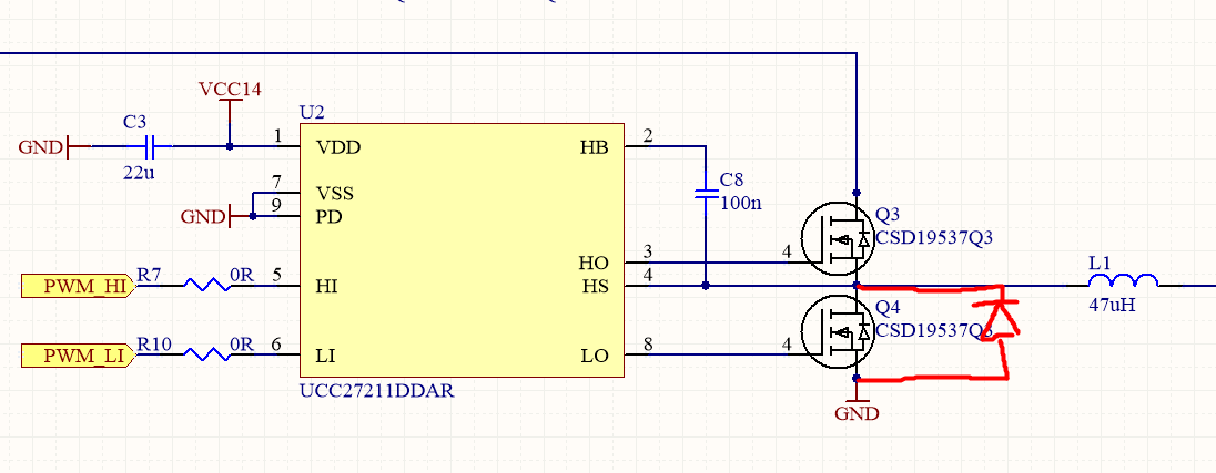
Diode is the SS510. This circuit works fine.

The problem is that Q3's body diode conducts from out to in when the mosfet driver is off. In our application this is not acceptable.

So ideally we would want the high side mosfet circuit to be bi-directional (back to back nmos). But it seems this driver can not handle that. Any ideas and or recommendations to do this ?

  • Hello Thijs,

    The appropriate engineer has been contacted and will answer your question soon.

    Regards,
    Mateo
  • Hello Thijs,

    I am an applications engineer with TI and will work to answer your questions. I have looked at similar applications to confirm the correct the back to back MOSFET implementation, but I need to confirm this will work in your application with the low side FET.

    I will continue to look at this application and update you soon. In the short term you can look at Figure 18 in the TPS2411 datasheet http://www.ti.com/lit/ds/symlink/tps2411.pdf to see if this will work for the high side MOSFET.

    Best Regards,

    Richard Herring

  • Driving the low side mosfet is no issue. Plenty of solutions for that. For now just focus on making the high side one bidirectional.
    Is the above circuit capable of accepting pwm of like 200kHz? the rise times is 10-20 times more than the current driver. This will have effect on efficiency.

    Would one of the following suggestions make this simpler?

    - Would an HV rail solve issues?

    - Would controlling the low side mosfet differently solve any issues?

    - Would an isolated supply solve any issues (keeping the increased cost and footprint in mind)?

  • Hello Thijs,

    For the reverse current protection on the high side MOSFET two N Channel MOSFET's can be driven with a common source configuration from the same high side driver. The high side switch is connected as the normal high side with VIN to the drain, gate to the driver, and source to the driver HS pin. The reverse bias protection switch is connected with the source common to the high side switch, gate to the driver, and drain to the power train switch node and low side switch drain. Both switches can be switched on and off with a common VGS applied but there are some details to the switch transition to consider, for this reason it is recommended to have separate gate resistances to be able to slightly adjust the turn on/off timing.

    During turn on, if the highs side switch turns on slightly before the reverse bias switch, there will be a short time of conduction of the reverse bias MOSFET body diode. If the reverse bias switch turns on first, there should be no consequence since the high side will be off.

    During turn off if the high side turns off first, and there is a reverse bias condition, there may be some conduction of the high side body diode back to VIN, but this should be a short time period. If the reverse bias turns off first during normal CCM operation, the HS pin of the driver will clamp to ground instead of a diode drop below ground since the body diode of the reverse bias switch will negate the negative voltage of the low side switch body diode; this should not be a concern however.

    One question would be, what will clamp the drain of the low side switch in the reverse bias conditions that you expect? If the power train switch node is not clamped to the input, you may need a snubber or clamp to limit the voltage.

    Regards,

    Richard Herring 

    Visio-App diagram_bidirectional.pdf