This thread has been locked.

If you have a related question, please click the "Ask a related question" button in the top right corner. The newly created question will be automatically linked to this question.

SG2524: PWM outputs

Part Number: SG2524

Hello,

My question is concerning the the generation of a PWM signal based on the value of the COMP pin on the SG2524. Basically what I want to do is to have an increased pulse width on my output when the value of the COMP pin increases and a smaller pulse width when the value decreases.

Suppose I want to do this with transistor Q1 on the SG2524. How should I connect the collector and emitter pin of the corresponding transistor? My first guess woul be in a common collector configuration. This would be with the collector pin of Q1 to the 5V reference and the emitter to ground through a pulldown resistor as in figure

Is this correct? If not how can I achieve this?

Thanks and bests,

Gabriele Ulissi

  • Hello Gabriele,

    Thank you for your question.

    There is a sawtooth waveform generated by the CT(timing capacitor) which gets compared against the COMP signal to generate the duty cycle. Now, then the COMP signal decreases the width of the pulse ie Duty Cycle increases and vice versa explained in the diagram. Now, this occurs internally in the SG2524 IC, however, if you want to achieve the same externally you will have to make sure to supply a Sawtooth wave in sync to the switching frequency and your COMP ref voltage 3.5V in the case of SG2524 to vary your duty cycle.

    Thanks,

    Sonal

  • Hi Sonal,

    Thank you for your answer. So as far as I have understood increasing the value of the COMP pin will decrease the duty cycle of the internal transistors.

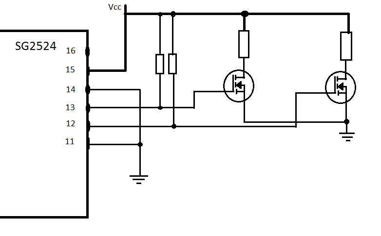
    Assume I want to switch two external MOSFETs with a duty cycle proportional to the value of the COMP pin. So I want this duty cycle to be maximum for COMP = 3.5V and minimum for COMP = 1V, which are the threshhold voltages of COMP according to the data sheet.

    Would the connection shown in the figure be able to satisfy this?

    Thanks,

    Gabriele

  • Hello Gabriele,

    I don't see any issues in the above connection since SG2524 is voltage controlled the COMP signal will determine the duty cycle just fine.

    Also, Just to bring to your view that the only difference between the COL 1(Pin 12) and the output of your transistor connection will be that, when COL1 is high the transistor will pull it down. So you will have the inverted switching waveform. 

    I hope that answers your question.

    Regards,

    Sonal

  • Hello Sonal,

    Everything seems to be clear now. Thanks for clarifying.

    Bests,
    Gabriele