Other Parts Discussed in Thread: PMP10703, LM2733
Hello all
I want to design power supply for gate driver IC of IGBT module (Three phase bridge).
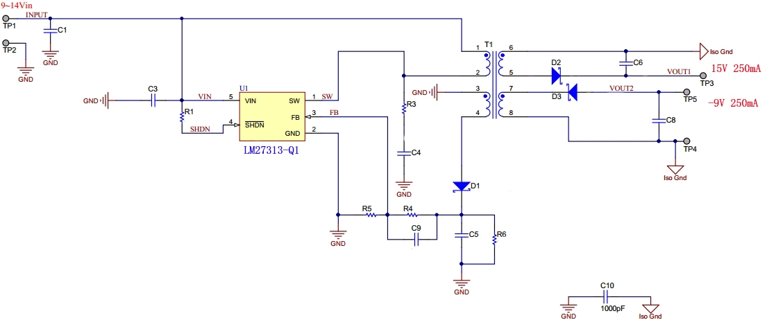
So I want to use LM27313-Q1 to design flyback convertor which can output 15V(250mA) and -9V(250mA).
This is the circuit topology I designed:(I'm going to design six same power supplies for gate driver ICs due to functional safety)
Q1: Is this power topology designed to be reasonable?
Q2:Is 250mA current output capability enough for this gate driver IC:1EDI2010AS?
Q3:Is there anything else I need to pay attention to?
Q4:Does TI have any better design topologies than my design?Such as more appropriate chips(automobile grade) of TI or more appropriate topology for this ?
Thank you

