This thread has been locked.

If you have a related question, please click the "Ask a related question" button in the top right corner. The newly created question will be automatically linked to this question.

TPS563208: Audible noise from the DC/DC Convertor

Part Number: TPS563208

Hello TI,

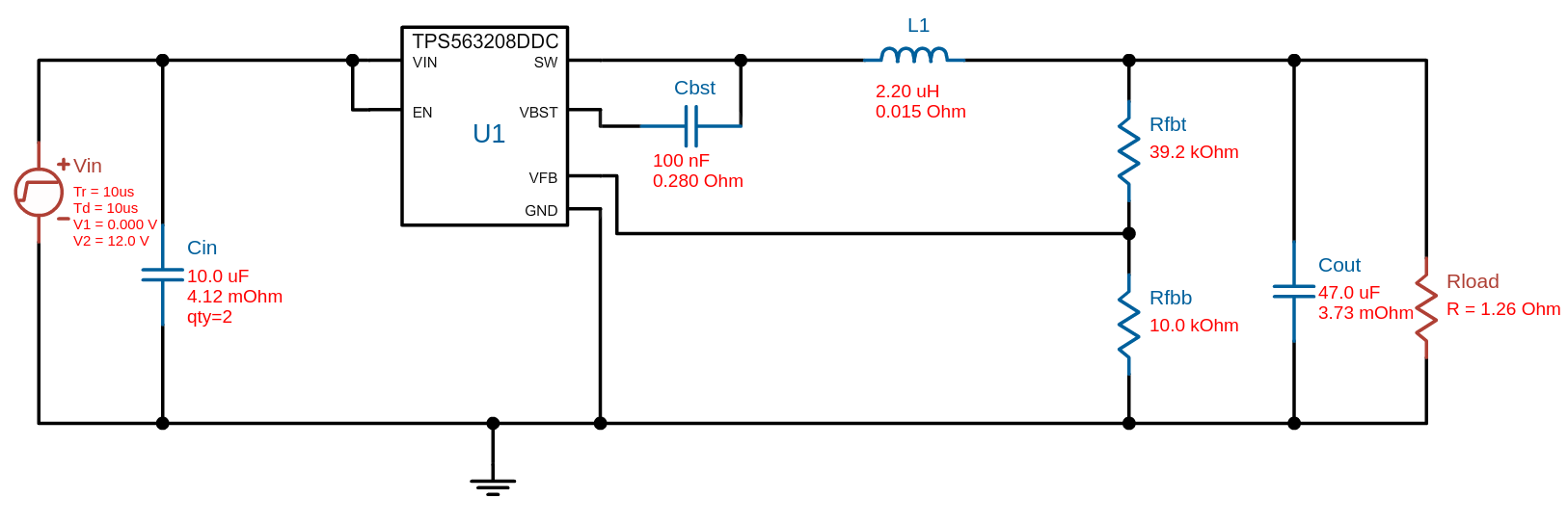
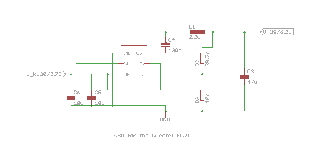
we are using the TPS563208 to step down 12V to 3.8 V to power a Quectel EC21 Modem. Please find attached the schematics as generated by the TI design tool. 

Cout 47u C-EUC1206 C1206 CAPACITOR,6.3 V, ± 10%, X6S

2 x Cin 10u C-EUC1206 C1206 CAPACITOR, 25 V, ± 10%, X7R

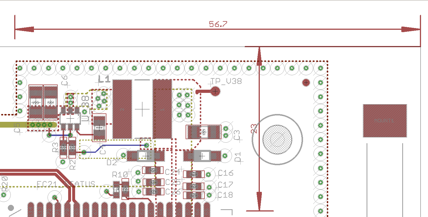
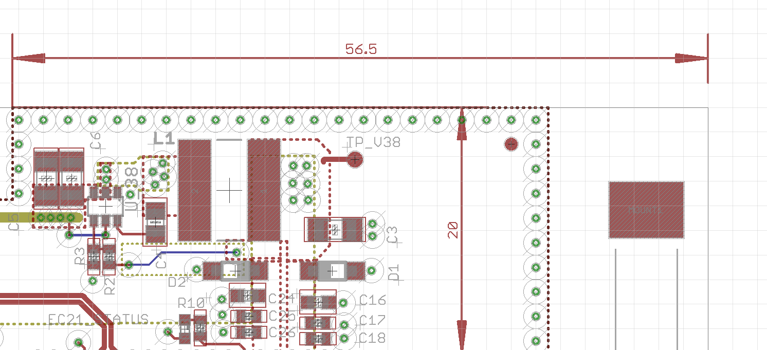
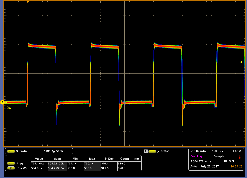
With our first prototype using the same schematic no audible noise was observed. However with the second prototype with a different Layer thickness, we are observing audible noise from the device especially when the modem is sending GSM data. The modem datasheet specifies a voltage drop of upto 400mV during such transmission bursts.

1. Is the noise from the MLCCs 'singing'? I've read this note form TI but I'm not sure any of the recommended solutions could work for us. Would moving the capacitors to the edge help?

2. How can I be sure that this singing is not from the inductor?

3. Do you forsee any long term functional problems if this singing is not eliminated?

Thank You!

  • Hi

    Did the two prototypes have same circuit design and use same external components? if yes, then problem should be caused by layout. improper layout will cause unstable switching and inductor may produce audible noise. pls upload the layout for checking.
  • Hello Andy,

    Thanks a ton for your prompt reply. Sorry it took me a while to get back to you. 

    Here are the actual schematics and layout. 

    The new prototype uses the same schematic, the only difference being the size of the board has increased by around 3mm on one side and there is a new hole in the vicinity. 

    The new prototype also uses a different layer build up. The thickness of the different layers in the PCB were adjusted to ensure impedance control where required.

    The third layer in the PCB is the VCC layer which is also used for the switching signal. 

    The external components remain the same, but I cannot be sure that they're from the same brand.  

    I'm not if this info is sufficient for your analysis, if you need anything else, please do let me know.

    New Layout

    Old Layout


    Commn Schematics for both  prototypes


  • Hi Pradeep,

    For your three questions:

    1. Is the noise from the MLCCs 'singing'? I've read this note form TI but I'm not sure any of the recommended solutions could work for us. Would moving the capacitors to the edge help?

    A: If the noise is from the MLCC piezoelectric noise, then moving the caps to the edge will help. I would recommend you to change the cap value or switch to NPO(COG) caps to try first to see whether they are the noise source. If so, change cap value or change layout is necessary.

    2. How can I be sure that this singing is not from the inductor?

    A: To check it, just see the waveform of SW and if the switching frequency is fixed and stable, the noise is not from inductor.

    3. Do you forsee any long term functional problems if this singing is not eliminated?

    A: It depends on the application and the feels of the end users. It is not good to hear the noise and TPS563208 is a fixed frequency part that should be out of audio noise. In this case, I think we could figure out the source, either inductor or caps. Thanks!
  • Hello Anthony,

    thank you for your reply. 

    I shall check with an Oscilloscope if the switching waveform is fixed and stable. If yes, then as you suggested I can rule out the inductor being noise source.

    If the noise is then Piezoelectric noise, then I could try replacing the MLCCs with C0G caps. 

    However since the same components work flawlessly on the previous prototype, I'm guessing the noise source has to be mechanical. The capacitors are now farther from the edge, maybe that's the issue. Also the hole in the board, maybe that disturbs the structural integrity somehow?

    Thank you for the support. 

  • Yes, agree with you. Cap singing due to piezoelectric noise could most likely the cause. Changing layer thick could lead to this kind of cap singing issue. Soft reminder, COG cap will be very expensive. Maybe it is better to consider to try different cap value.
  • Hello Anthony,

    The switching frequency oscillates between 560-580kHz . Please find below the screenshots from the oscilloscope recording the switching frequency waveform.

    Is this stable enough? Or do you think the auidble noise could be from the inductor?

  • Hi Pradeep,

    The oscillation or jitter should be normal here. The frequency is around typical. I don't think inductor is the noise source.
  • Hello Anthony,

    Having ruled out the inductor as the source of noise, I'm looking at alternative capacitors now.

    I've been unabled to find any C0G capacitors in the uF range easily. Can I try using two 22uF X7R capacitors instead like on the EVM?

    How does changing the total capacitance affect the transient response/output voltage ripple? I read the datasheet recommends any value between 22uF and 68uF. So two 22uF caps should be ok right?

    How about Tantalum capacitors in the 47uF range? I know they're going to be much more expensive, but if I could get rid of the acoustic noise we will be done with the development finally!

    Thank You!
  • Hi Pradeep,

    Yes, you could try one or two 22uF X7R cap like EVM. Have you checked on the load current or inductor current? I am also suspected that your load may have some oscillation that is around audible frequency. Please also check.

    Also, could you let me know how you debug out inductor is not the source?
  • Hello Anthony,

    thanks for the prompt response.

    "Hi Pradeep,

    The oscillation or jitter should be normal here. The frequency is around typical. I don't think inductor is the noise source."

    I assumed the inductor was not the noise source based on your previous reply. Do you think the inductor could still be a noise source even though the waveform is stable?

    The funny thing is if the PCB is provided enough cushioning the noise is barely audible. This is one other reason why I assumed the noise is from the piezoelectric effect on the cap. 

    What should I look for in the inductor current waveform?

    Thanks again!

  • Hi Pradeep,

    Sorry that I missed the information that you mentioned the SW waveform is stable. If the SW waveform is stable, then inductor is not the noise source. The reason why I brought up inductor current waveform is that I am worried that your load is not stable. If the load is fast changing, the SW waveform will also show big jitter which could be in the audible frequency range. If SW is stable, then it is fine. Please go ahead to investigate on capacitor noise and try different cap value. Thanks!

  • Hello Anthony,

    I tried something unconventional. I desoldered the VOUT capacitor from the board and connected it off the board with wires. This is of course not the optimal layout, but I wanted to decouple the capacitor from the board mechanically. It doesn't make that much of a difference. Either the noise source is some of the smaller capacitors we have further from VOUT to the EC21.

    Or the the inductor might be the noise source. Is it sufficient if I check the switching voltage waveform under rapidly changing load?

    If the inductor is the noise source, then would changing the inductor to another component work? Or do the capacitor values have to be changed?

    Thanks for your support.
  • Hi Pradeep,

    Sorry for the late. Have you tried to turn on the persist function on the scope to capture the SW waveform? It will show the SW jitter in a long time scale.