


Other Parts Discussed in Thread: LM3488
Hi Team,
We are working in one battery powered project, where device will take power input from Vehicle battery (Vin = 8 ~ 16V) and require 12Vdc as output. For such kind of buck-boost configuration we have used LM3488Q-Q1 IC in design.
Below I have pasted image of schematic design. Kindly review.
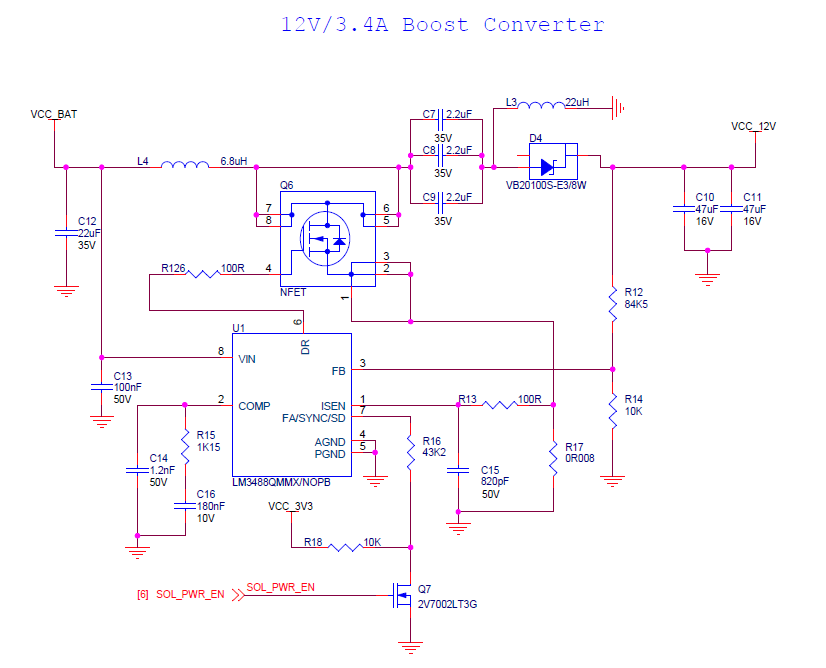
We have gone through the layout guideline provided in datasheet, but it has described point when application is in Boost mode. Taking that as reference we tried to make current loop from L4-Q6-D4 as small as possible. Above that below are some point where we require your inputs:
1. Is there any special requirement in placement of L3? Do we need to consider loop involving L3 for AC noise reduction?
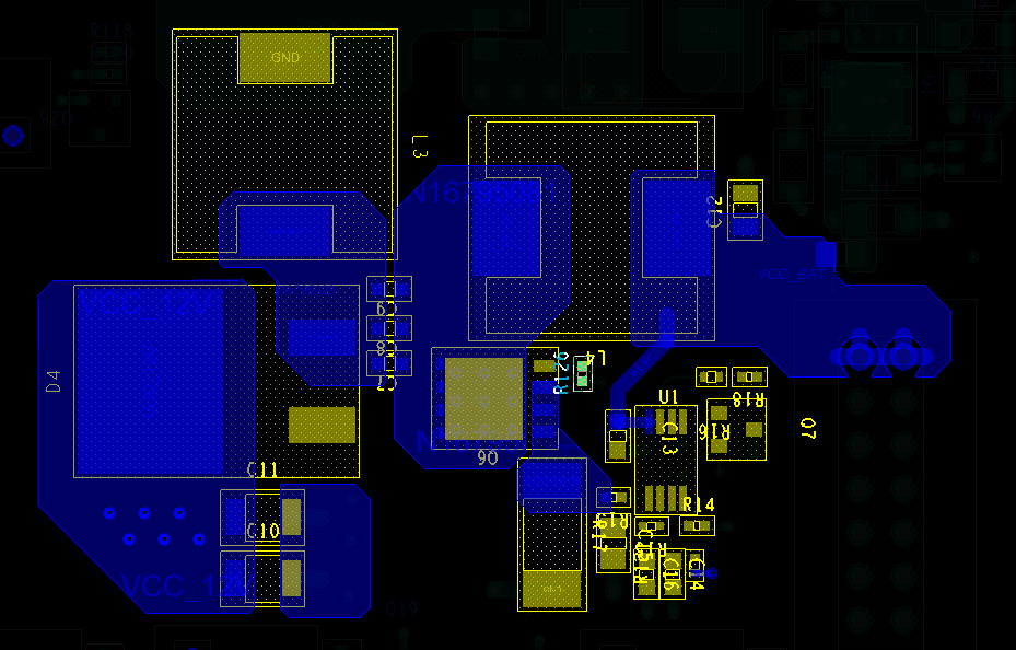
2. In reference layout, they have tried to make GND shape common on top side for IC & its associated by providing vias for DR (pin#6) pin & VIN (pin#8) pin connection with its discretes.
Is it OK to have vias for such switching nodes & power inputs?
3. Any other recommendations, which we need to take care during placement & layout?
Below added image of component placement done for LM3488 IC:
Let me know if require any further detail for review.
Thanks,
Dhvanish Parekh
