This thread has been locked.

If you have a related question, please click the "Ask a related question" button in the top right corner. The newly created question will be automatically linked to this question.

TPS54240: Instability due to compensation pin

Part Number: TPS54240

Hello,

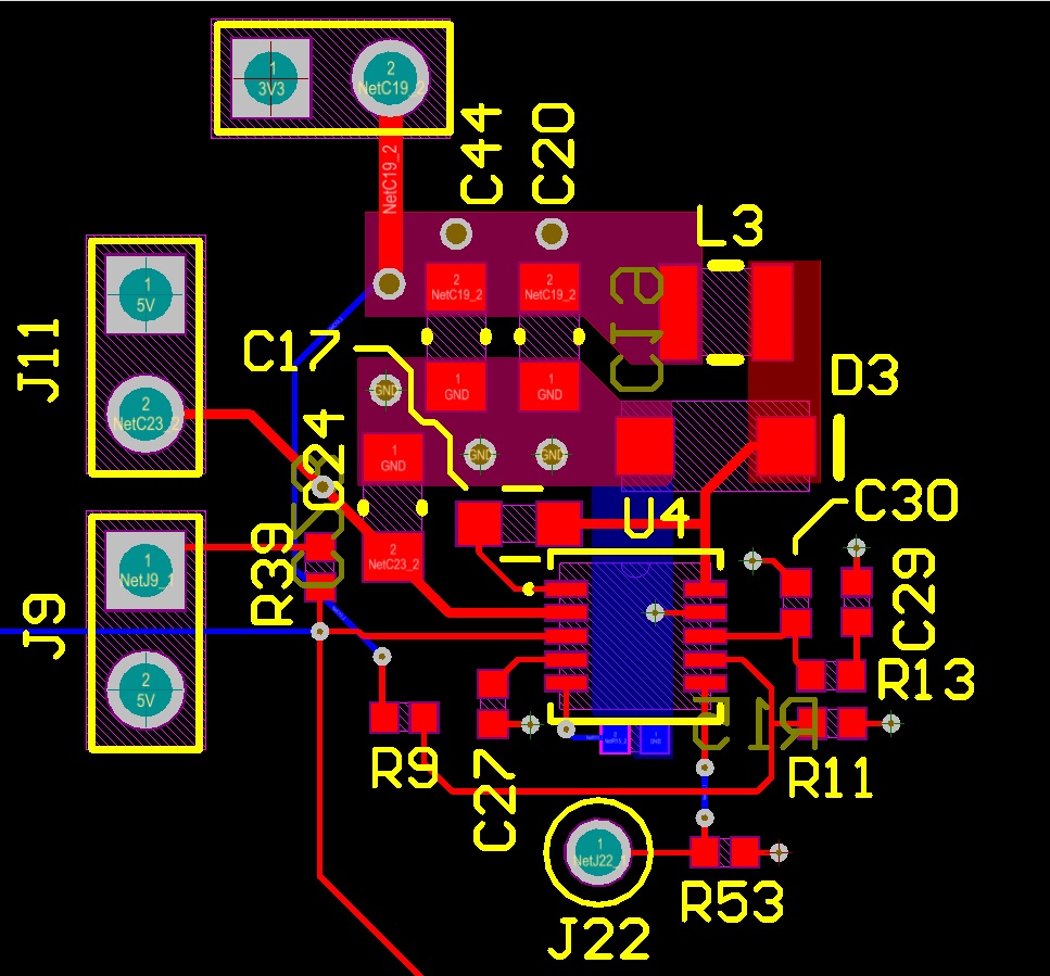
I am designing a buck regulator shown below.

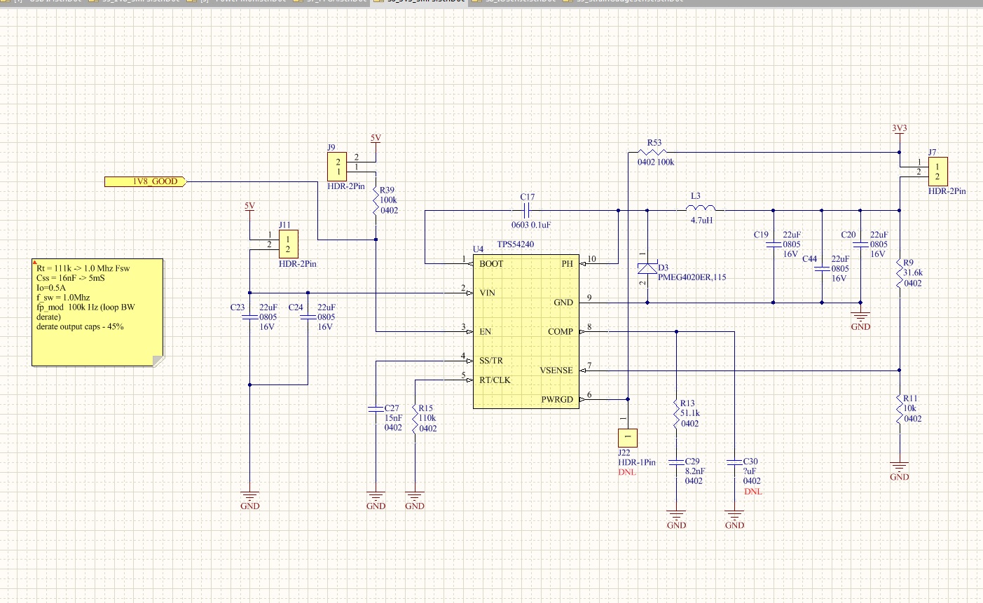
The jumpers J11 and J9 are installed.  C30 is not installed, I just put the footprint on the board.  J7 is not installed so the load doesn't affect the supply yet.  I simulated this in tina with a step load etc...and it looked fine.  Unfortunately it is not working on my board.  R13 and C29 are installed.  

Could someone elaborate on how I've gone wrong with the compensation network?

Thanks!

  • Please define what is not working?
    Also, please send any voltage waveforms of the switch pin and a snapshot of you pcb layout
  • I apologize.  Not working as in doesn't regulate to 3.3V but ~2.8V instead.  If I remove the RC components on the comp pin it regulates at 3.3V fine.

    I've attached the layout here.  I will grab some waveforms today.  Thank you for the reply!

  • Frank,

    I was mistaken.  This circuit is not regulating correctly under load in this configuration either.  I initially though removing the compensation components allowed  the device to regulate  at  the expected 3.3V and it does but only without  a load attached.

    These screenshots were taken with the design described above with NO compensation components loaded.  The  top (blue) trace is the output and the bottom (green trace) is the PH pin (pin 10) of the TPS54240.  

    Below is the key describing  the configuration of the circuit each screenshot was taken in.

    LeCroy13.png - Screen shot of the circuit  with no load  and no components connected to the COMP pin.

    LeCroy14.png - Just a  second screen shot with the same  configuration as LeCroy13.

    LeCroy15.png - Same probe points, but the output of this regulator now has a 7.5 ohm load.  Nothing is connected to the COMP pin.

    LeCroy13

    LeCroy14

    LeCroy15

  • You will need to connect the DAP to the ground plane. I assume that the device is on the top, but I do not see the ground plane on top
    attached to the DAP. This is a very important ground connection.
    You will also need to use wide traces, if not large fills, for the following signals: gnd, pgnd, vin, sw and boot.
    Also, use a ground fill/plane on top.
  • Is the DAP the thermal relief ground pad on the bottom of the IC? I unfortunately overlooked that in the footprint so I don't have that pad on these boards.

    I've noted your recommendations and will implement them on the next spin. Do you think those items could be causing the above issues? Do you have any insight regarding the COMP pin?
  • Yes. This is a very important electrical and thermal connection that must be grounded.
    From you sw waveform at load it looks like there is a lot of droop in the waveform.
    This may be from the resistance of the very narow traces that I mentioned above.

    Not sure about the comp components making a difference, however you will need a better layout
    first. Then if the system is unstable you can adjust the comp values.

    The comp components and FB resistor must be ground at the gnd pin of the device, like the example on the data sheet layout.
    Then that gnd is connected to the DAP.