Other Parts Discussed in Thread: LM5176
谢谢:
我遇到的问题分两种电路来描述
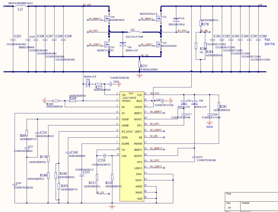
一:TI推荐电路,参考webbench。输入电压16V~40V,输出21V/7A电路。
1:输入16V,输出21V,输出电流加大到6.4A时,LM5175会损坏。如附件图16V输入,21V6.4A输出的各位置波形。
2:输出21V/3.5A,输入电压从16V加大到19V时,LM5175会损坏。如附件图19V输入,21V3.5A输出的各位置波形。
由于在第一种状态内发现,在6.4A负载时,左边上管和下官驱动有变化。为了排除问题,故先看boost状态是否正常。所以有了第二种情况:
二:(TI推荐电路,参考webbench输入电压16V~40V,输出21V/7A电路)这个电路的基础上,并把左上管DS短接、左下管取掉。图形见对应附件
1:输入16V,输出21V,空载,左下管和左上管互补导通,左下管和右下管某些时候同时导通。(不符合我们对BOOST的理解:认为左下管不应该导通,左上管应该长通)。
2:输入16V,输出21V,1A负载,左下管关闭,左上管长通,右下管脉冲导通关闭。(符合我们对BOOST的理解:认为左下管不应该导通,左上管应该长通)。
3:输入19V,输出21V,1A负载,左下管和左上管互补导通,左下管和右下管某些时候同时导通。(不符合我们对BOOST的理解:认为左下管不应该导通,左上管应该长通)。情况跟空载相近。
损坏之前伴随着啸叫,没有发热现象,经常坏LM5175和左上管和左下管。
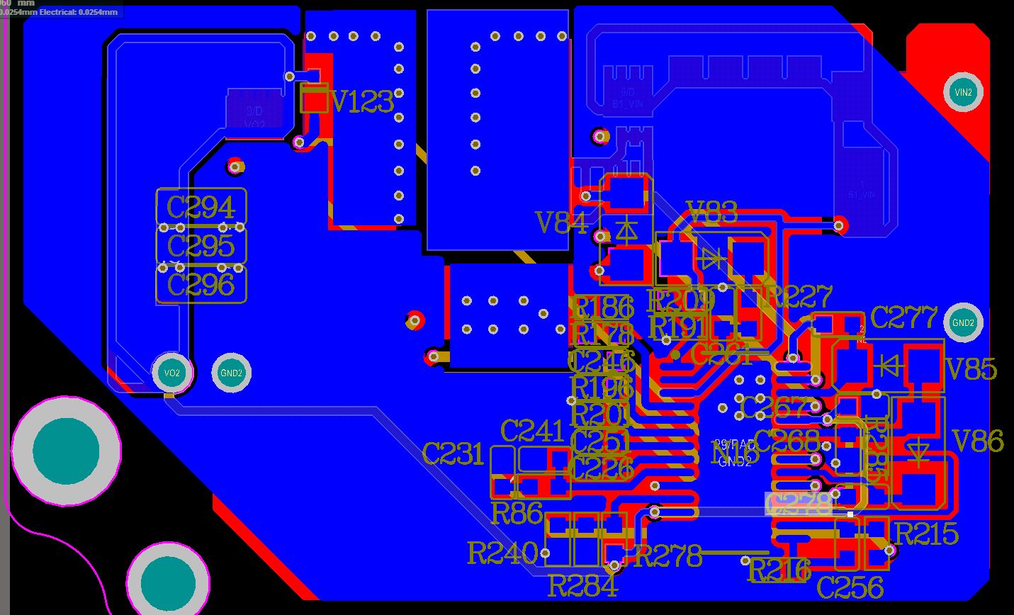
顶层:
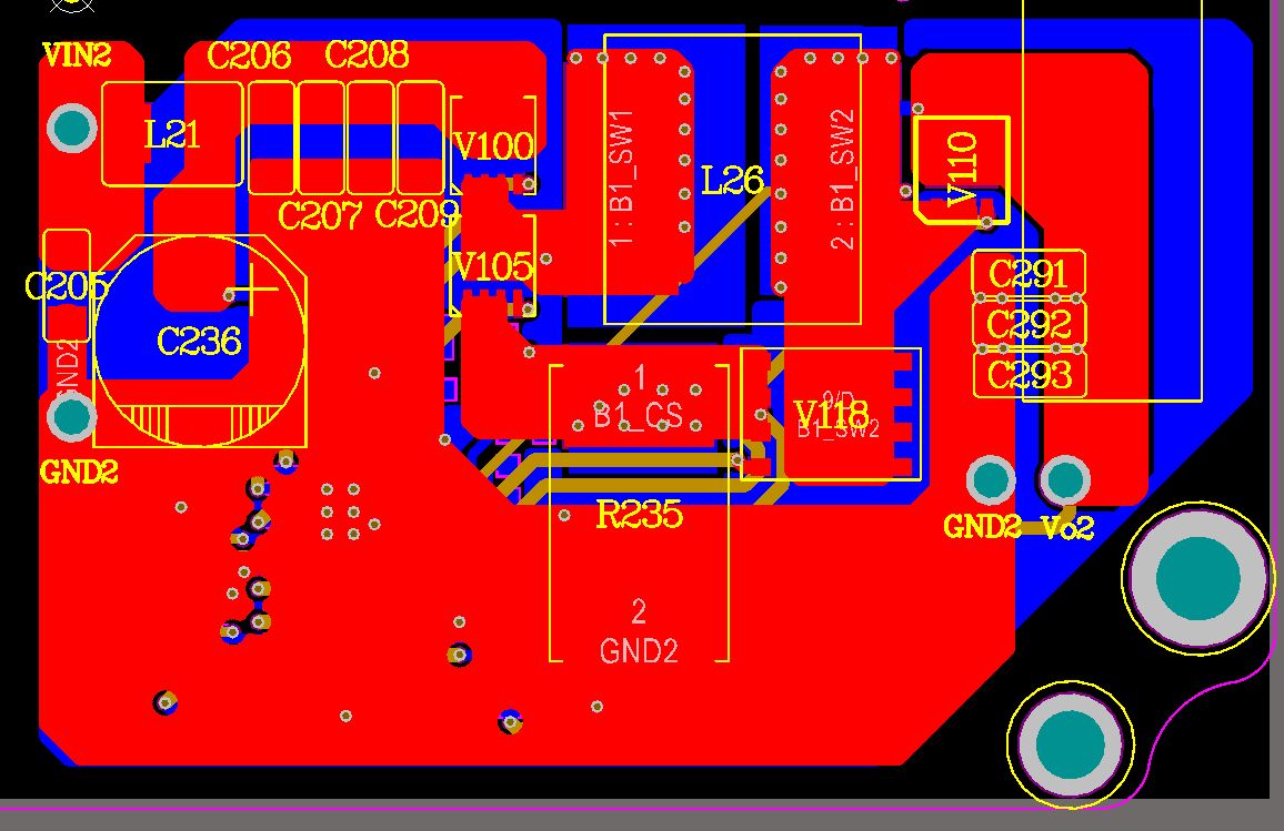
中间层:
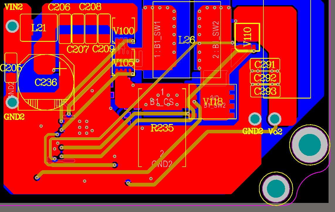
底层:
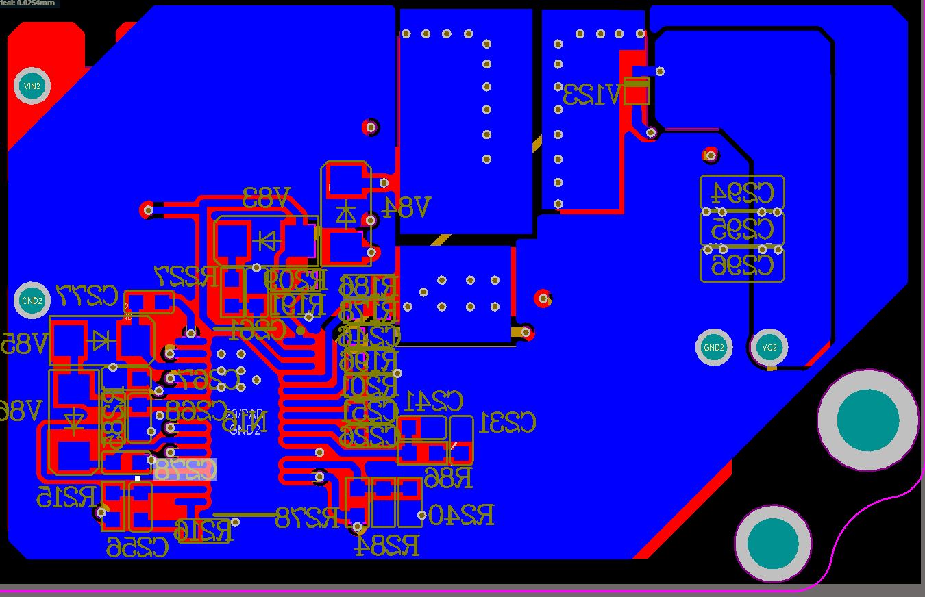
底层-镜像:
采集的波形:
第二电路:输入16V输出21V1A负载黄色(20倍衰减)为HDRV1蓝色为LDRV1:

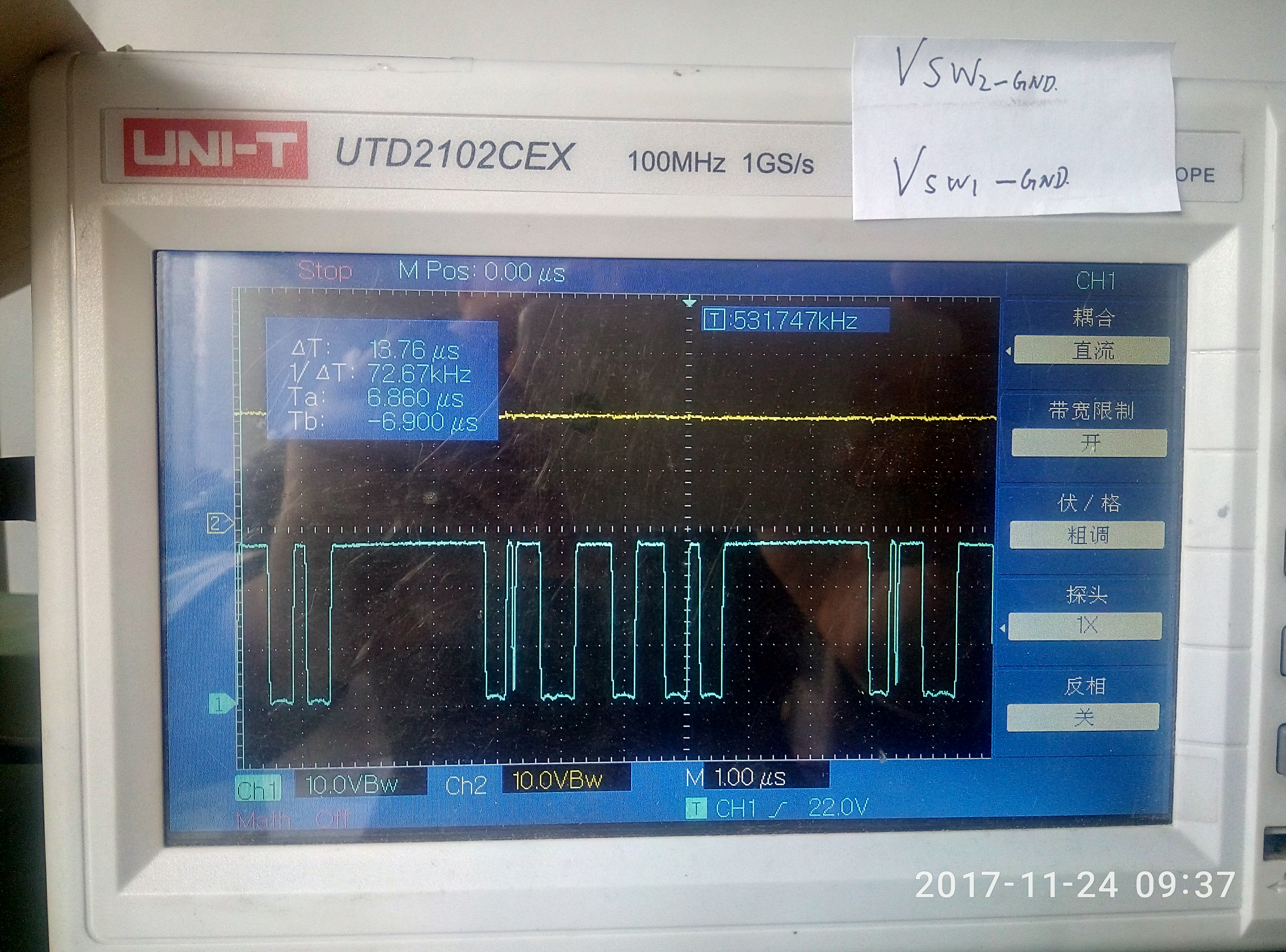
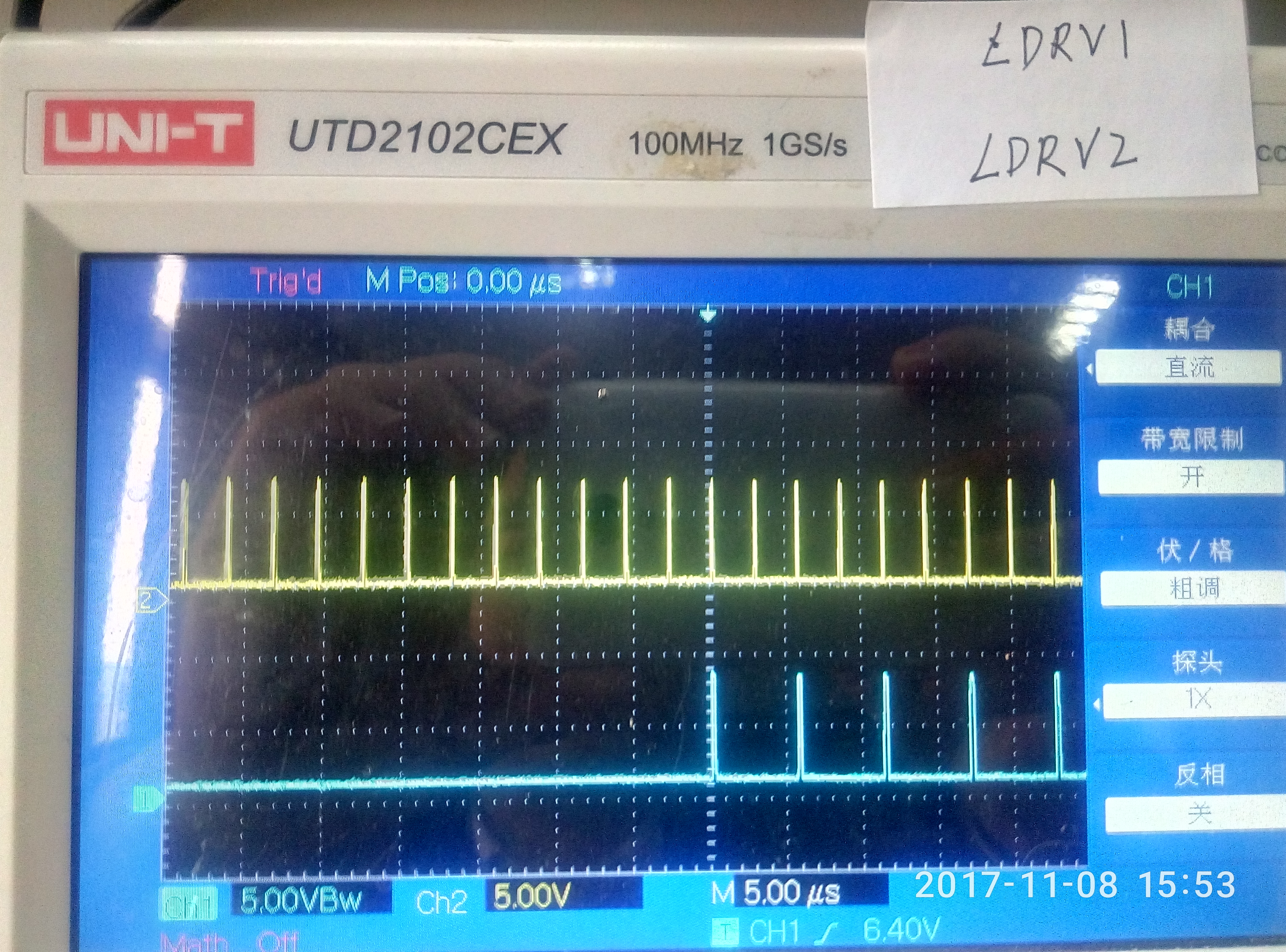
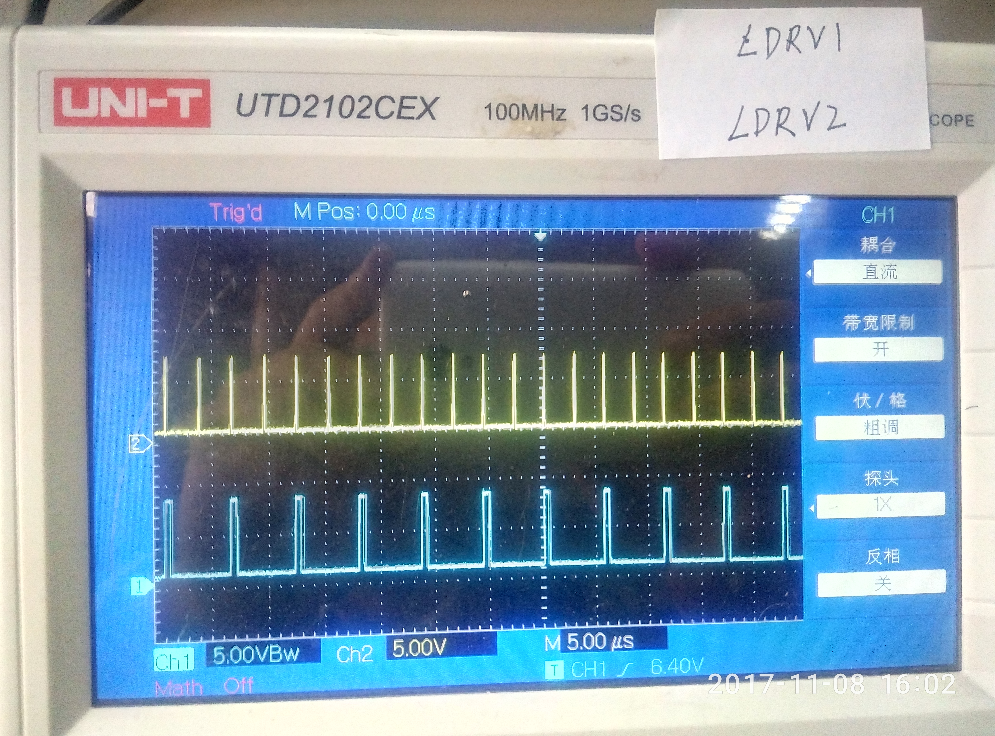
第二电路:输入16V输出21V1A负载黄色为LDRV1蓝色为LDRV2
第二电路:输入16V输出21V空载黄色(20倍衰减)为HDRV1蓝色为LDRV1

第二电路:输入16V输出21V空载黄色为LDRV1蓝色为LDRV2
第二电路:输入19V输出21V1A负载黄色(20倍衰减)为HDRV1蓝色为LDRV1

第二电路:输入19V输出21V1A负载黄色为LDRV1蓝色为LDRV2
第一电路:16Vin-21Vout6.4A-Vboot1_sw1

第一电路:16Vin-21Vout6.4A-蓝色为Vboot2_sw2黄色为右上管Vgs

第一电路:16Vin-21Vout6.4A-蓝色为左上管Vgs-黄色为坐下管Vgs

第一电路:19Vin-21Vout3.5A-Vboot1_sw1

第一电路:19Vin-21Vout3.5A-蓝色为Vboot2_sw2黄色为右上管Vgs

第一电路:19Vin-21Vout3.5A-蓝色为左上管Vgs-黄色为坐下管Vgs