This thread has been locked.

If you have a related question, please click the "Ask a related question" button in the top right corner. The newly created question will be automatically linked to this question.

TL494: How do I setup a 20 kHz pulse wave with 50% duty cycle with this part?

Part Number: TL494
Other Parts Discussed in Thread: LM555

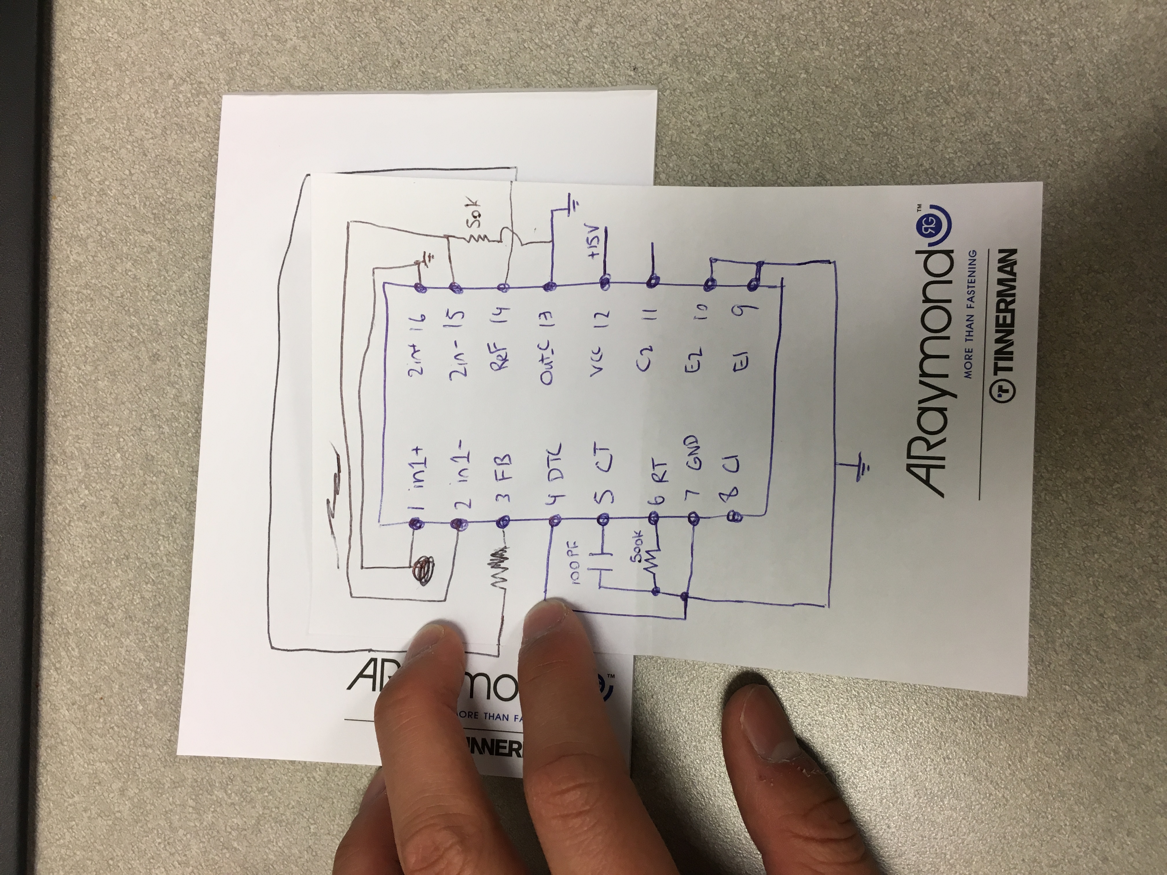
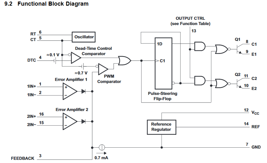
I know in the datasheet that it requires the IC to have CT and RT connected with equation 1/RC = frequency so I have 100pF and 500K Ohms connected to CT and RT respectively. I have DTC grounded and Emitter 2 grounded. VCC is connected to a 15 V source and GND is connected to GND. C2 is my output and output ctrl is connected to ground to enable single-ended mode. Are there other pins I need to connect or can I just leave them as open. 
Again I am trying to set-up a 20 kHz frequency with a duty cycle of about 50%.  I thought grounding the DTC will give me a 45% duty cycle according to the datasheet but I get about 5/10% on my scope. How do I vary the duty cycle and how do I get it to output correctly. I left 2 noninverting and inverting inputs as open as well as C1, E1, Ref, and Feedback. Any tips/ explanation on how to proceed?

  • Hello

    I would suggest you ground E1 as well as E2. ( As a general rule, I don't like leaving pins floating because they can take up an uncontrolled voltage and cause unpredictable results - unless they are an open collector output)

    The reason you are getting a lower duty cycle than you expect is probably that the FB pin is floating up to a relatively high voltage -. You should connect the EA- and EA+ inputs as shown in the app diagram on Page 8 of the Data Sheet. this will set the outputs of the error amplifiers to zero volts. You should be able to control the duty cycle by putting a voltage on the FB pin from an external source. A pull up resistor to REF will supply the 0.7mA current - see the block diagram on page 10. To get 0.7V at this pin you should use a resistor of (5V - 0.7V)/0.7mA or about 6.2k. I haven't toleranced this value and you may need to experiment a bit.

    Please let me know if you need any more help.

    Regards
    Colin


  • Thank you for the information. Just to be sure, can you take a look at my quick sketch of what it should look like. I connected 1in+ and 2 in+ together and to ground as shown in page 8 of the data sheet. for 1in- and 2in-, I connected it to Output Control which I connected to ground from my original description but should I connect it to reference as in the page 8 schematic? Lastly, I connected Reference with a 6.19K ohm resistor to Feedback. Thank you for your help.

  • I tied the inverting and noninverting inputs to ground and messed around with different resistors for REFERENCE to FEEDBACK pins. When using resistor values higher or lower than 6.19K Ohms, I get a constant VCC value. When I use 6.19K Ohms, I get a slight increased duty cycle, maybe +2%, still not getting the desired duty cycle of 50%. Any possible solutions?
  • Hi

    Thanks for the schematic - I think I know what the problems are.

    1/ To program max duty cycle the FB pin must be held at a low voltage. To do this you need to connect IN1+ and IN2+ to ground and then IN1- and IN2- to VREF through a resistor - 50 k should be ok but the resistor value isn't critical. The point of doing this is to force the outputs of the two error amplifiers to zero. Then connect FB to ground via a 1k resistor (this value may need to be adjusted up or down). OR, use a potentiometer from VREF to GND and connect the wiper to FB. This will give you control of the voltage at the FB pin and of the duty cycle. OR, simply use an external voltage source to set the votlage at the FB pin. You have both the IN+ and IN- pins tied to ground so the amplifier output may be high or low depending on amplifier offset voltages. Also you have connected FB to VREF through a resistor - again this will tend to pull the FB pin high and give you a very low duty cycle.

    2/ You should use a pull up resistor on the collector of the output transistor. 10k to VCC would do for initial testing.

    The other connections look ok

    Please let me know how you get on

    Regards

    Colin

  • Thank you Colin, this was exactly what I needed. The potentiometer allows me to change the voltage which in turn change the duty cycle on the output
  • Hi

    Glad to hear that.

    Regards
    Colin
  • Just trying to understand what the circuit is doing a little more, can you explain why grounding in1+ and in2+ and then connecting the inverting inputs to VREF creates a output voltage of zero for the feedback? And then how does that influence the duty cycle?
  • Hi

    The TL494 device uses ‘leading edge modulation’ to set the duty cycle. The PWM output is held OFF until the PWM comparator trips and so the output pulse width varies from 97% of the period to 0% as the voltage present at the error amplifier output varies from 0.5 V to 3.5 V, respectively. An increasing voltage at the Feedback pin gives you a shorter duty cycle. The article at https://www.eetimes.com/document.asp?doc_id=1279671 gives a detailed explanation of the technique.

     In your case you don’t want the Error Amplifiers to have control of the duty cycle so we need to set their outputs low so that you can directly control the voltage at the Feedback pin by an external source. The voltage at the Feedback pin reverse biases the diodes at the error amplifier outputs of course.

    Setting the IN+ inputs to GND and the IN- inputs to REF forces the error amplifier outputs to go to GND leaving you free to set whatever voltage you want at the Feedback pin.

    Regards
    Colin

  • Thank you for the information. Can you tell me how this IC differs from the 555 timer and which IC is easier/more advantageous in what I am trying to do.

  • Hi

    Which is easier or more advantageous ? - that's actually a very difficult question to answer

    So: if the TL494 is working and doing everything you need, then I would continue to use it for the normal reason which is 'if it isn't broken, then don't fix it'

    The TL494 is a 16 pin device and will give you more flexibility than a LM555 - two outputs for example
    The LM555 is a 8 pin device so it will take up less space
    You should compare the prices you can get for the two devices - I can't give any advice here because pricing depends on your supply chain and many other factors.
    The LM494 will probably be more 'stable' over temperature for example than the LM555
    How much current do you need to drive the load at the IC outputs ?
    Are you prepared to re-layout your PCB to accommodate the LM555 ? and are you prepared to take the time to do that.
    Are there other important tasks that you should be doing rather than investigating and changing a working solution into another working solution - you may find that after looking closely at the two devices that the TL494 is actually the better choice.

    Regards
    Colin