Hello TI,
Our PCB layout is as follows
TOP: Signal + GND pour
2nd layer : GND
3rd layer : VCC
BOTTOM: Signal + GND pour
The VCC includes the V_33 polygon and V_38 polygon. The V_33 polygon covers most of the area on the VCC plane.
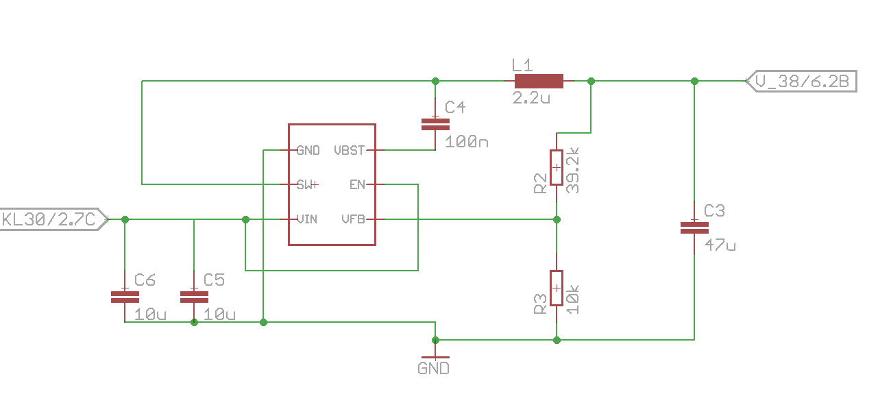
Please find below the schematics and layout for the 12V->3.8V circuit. The TPS563208 datasheet has the following guidelines regarding the feedback trace.
6. A separate VOUT path should be connected to the upper feedback resistor.
7. Make a Kelvin connection to the GND pin for the feedback path.
8. Voltage feedback loop should be placed away from the high-voltage switching trace, and preferably has
ground shield.
So, I start by using vias to route the feedback trace on the bottom layer.
Am I right in assuming that the return path of this feedback trace (which is on the bottom layer) will be on the VCC Layer?
In order to ensure that the noise from the return path (of the feedback trace) does not couple in the other power plane polygons in the VCC layer, I created a separate polygon called RETURNV_38 which connects to nothing at all and is simply present to ensure a clean return path for the feedback trace.
This seemed like a good idea a couple of months back, but now I'm not so sure. Since the polygon is not connected to anything at all, will this polygon even serve as a return path for the feedback trace? Is the feedback trace going to avoid this polygon and simply take the long way round this polygon?
I've read numerous application notes from Texas recommending NOT splitting the GND plane. Applying this logic, I think I might have worsened the EMC by including this specially designed polygon.
Apologies if my question is not clear enough. Simply put is it bad if the return path for the feedback trace is through the V_33 polygon?
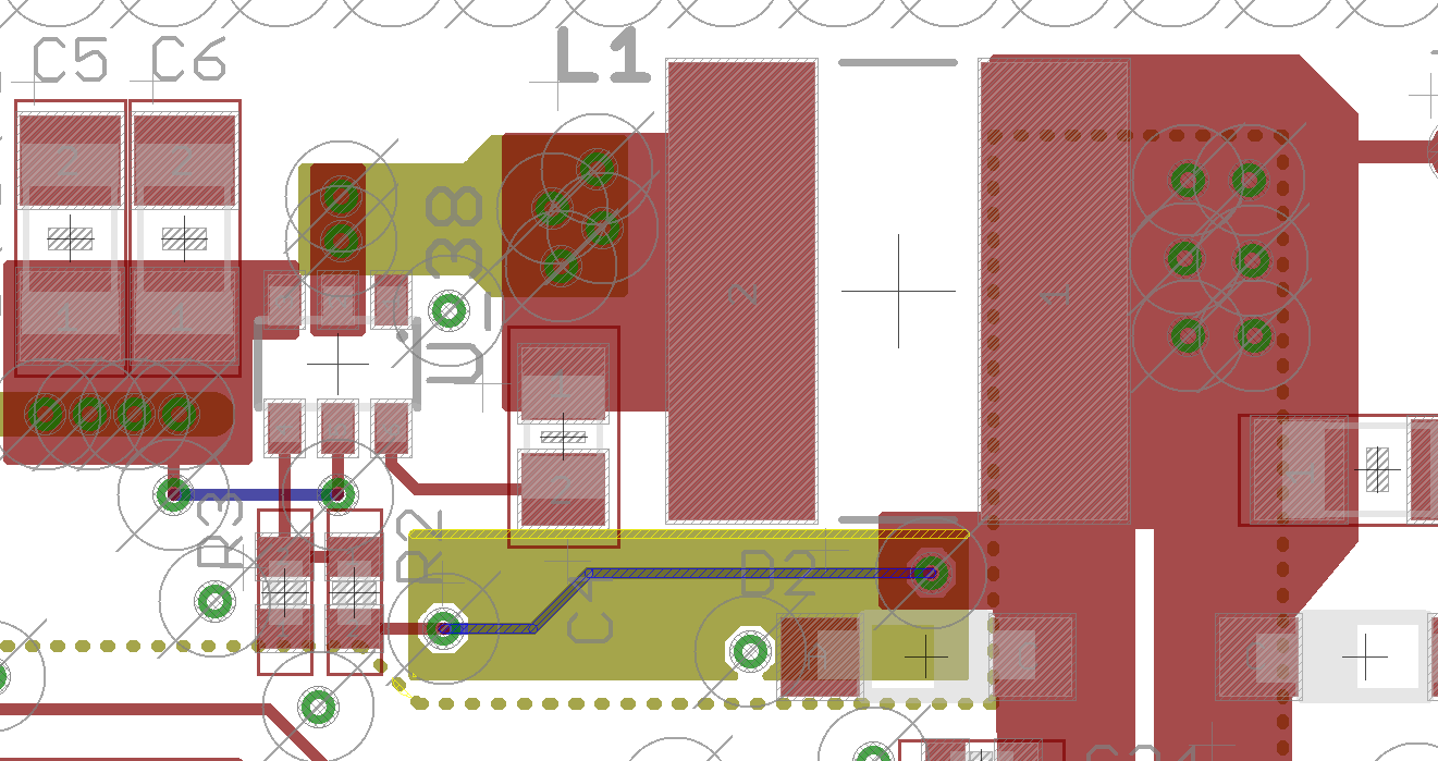
The layout below. Shown in red is the top layer. GND is a complete layer without any split.
VCC layer is yellow. Shown in the image below is the switching trace. Then the RETURN_V38 polygon. At terminal 1 of the inductor L1 is the output plane. The rest is V_33 polygon.