This thread has been locked.

If you have a related question, please click the "Ask a related question" button in the top right corner. The newly created question will be automatically linked to this question.

32KHz clock

Other Parts Discussed in Thread: OMAP3503, TPS65930

Hi!

I am using OMAP3503 with TPS65930.

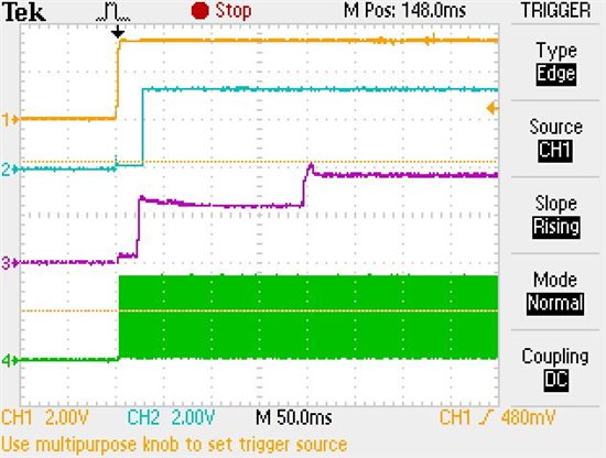
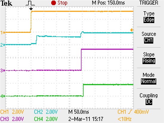
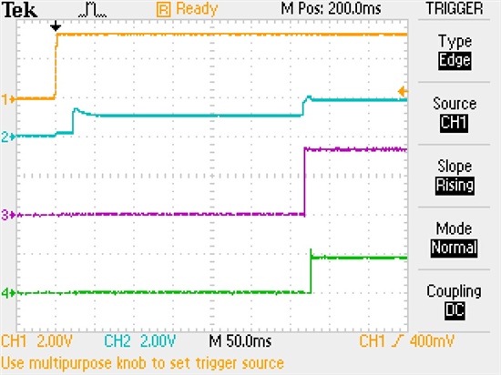
From what I observe, the 32KHz clock (TPS65930, 32KXIN at pin L14) does not start until ~250ms after +3.3VDC supply voltage becomes valid. My application requires a faster start-up time (less than 100ms) and a 32.768KHz crystal is used at the moment.

I would like to confirm that it is possible for the 32KHz start-up to be that long before considering using an external 32KHz oscillator instead to improve start-up time. If an external oscillator is used, what is the voltage level expected - +1.8VDC or +3.3VDC? I am assuming no voltage will be produced at VDD1, VDD2, VIO, etc OUTPUTS until this clock is seen at 32KXIN.


Please advise.

Thanks.

  • Hi,

    That is the approximate start-up time.

    For an external oscillator you will need 1.8V. Please see the details in the data manual.

    Yes, 32K has to be running and stable before you can see the DCDC's powered up.


    Regards,

    Gandhar.


  • Since TPS65930 relies on a stable clock before DCDC's power up, does that mean we need an independent external +1.8VDC to power up the external 32K oscillator?

  • Hi,

    Yes, thats correct.

    This can come from a voltage divider from the main battery supply. I dont think you would need an external LDO for this purpose.


    Regards,

    Gandhar.


  • Hello!

    The clock will require a proper regulator to work. Simply using a voltage divider will not provide a good clock source (proven in lab).

    This is what I get after using an external oscillator for the 32KHz.

    However, it is observed that the output voltages still takes a while to get to stable values. Why is there a step on waveform (3)?

    Included here is the plot:

    1. +3.3VDC

    2. IGNORE

    3. +1.8VDC output from TPS65930 to OMAP3

    4. 32KHZ clock


    Thanks,

    Sieow

  • Hi,

    It will help if you can provide a plot with input, REGEN, VIO and NRESPWRON. I dont think your board is powering up as expected. The power should be done in less than 10msec or so. You can add up all the delays in the data sheet.

    VIO reaching its expected level in more than 150msec is very strange. It will help to see the complete power-up sequence to understand what i shappening on your system.


    Regards,

    Gandhar.


  • Here is the plot:

    1) +3.3VDC VIN

    2) +1.8VDC VIO

    3) REGEN

    4) NRESPWRON


    +1.8VDC with respect to +3.3VDC does not make sense. The rest of the signals do follow the spec sheet timing for sequencing once the chip gets up to its feet i.e. when REGEN starts.

  • Hi,

    There is a delay in stabilizing the 32K even if you are using an external signal. The internal oscillator cannot be bypassed and hence you see the delay. With an external 32K the delay will be lesser than with using a crystal.

    The VIO step you see would be due to the leakage on the internal power domains. The 32K in the device is on the VRTC domain (1.5V). The external 32K you are using is 1.8V. When you use a crystal there is no mis-match between domains. I dont know the source of your 32K. You can try with a 1.5V 32K to eliminate the step. 

    I hope this helps.


    Regards,

    Gandhar.


  • Hi!

    The following plots are taken with TPS65930 using crystal for 32K (NOT oscillator) and the step on +1.8VDC is still there.

    1) +3.3VDC

    2) +1.8VDC

    3) REGEN

    4) NRESPWRON

    Top figure: Power off, wait for a few seconds, power on

    Bottom figure: Power off then power on immediately

    Note that the time for the device to come up also varies. Most importantly, the +1.8VDC "leakage" (step) is still there. Note that for these plots I am using crystal so there is no mismatch that could possibly leak all the way from 32K in to VIO (+1.8VDC) output.


    Can your team do similar measurements on your side? The TPS65930 is used to power up OMAP3503 on our side.

  • Hi,

    Please see the figure attached. This was on a standalone board. I do not see any step on VIO rail. The VIO rail shows a slight ramp at th ebegining, this is due to the 32K ramp. This board uses a crystal for 32K.


    Regards,

    Gandhar.


  • Hi,

    Aaron sent me another email for an update. Here is what I replied to him. I got an OoO from him, he is traveling and may get back to you a bit later.

    Schematics look fine to me. Something on their board is loading/leaking on the VIO output. Is it possible to isolate VIO on the platform?

    I know this can be tough and IO goes at all places. But I cannot think of any other better way to see how we can isolate. If the traces are on top layer then they can try to cut the trace that provides 1.8V output.


  • Gandhar:

    I was looking into isolating VIO to detect why we have a 1.5-1.8VDC step during start-up. We do not have any traces for it on the top/bottom layers. Nonetheless I will see what we can do here. Might be able to drill and scrap a board.

    At the mean time, I have a few questions for you.

    1) What is the worst case timing over operating temperature for REGEN startup when crystal is used? This timing parameter will allow us to characterize the worst case start-up of our system.

    2) What is the min loading for all TPS outputs? I did not see any requirement for it in the datasheet. For example, what we observed is that VIO = 1.92VDC during reset (very little loading) and +1.8VDC after reset (normal loading). A loading resistor in the range of 100ohms to 900ohms seem to stabilize VIO at +1.8VDC at reset and after reset.

    Thanks.

  • Gandhar:

    Good news! I found the leakage from a level translation chip we have downstream from this card. The step issue is resolved.

    Hope to hear from you regarding question (1) and (2) above.

    Thanks!

  • Thanks for the update.

    The power up sequence is same under all conditions. It depends on the crystal when it stabilizes. Once the crystal stabilizes then the powerup will be normal. There may be dependency on the external crystal but not on the internal oscillator circuit. I dont understand your question or the specific need for this timing.

    Also, ideally there is no loading required. On my test board I power-up the dvice without any load an dit does regulate as expected. 

    Since you found the problem now do you still need to know loading, as said above there is no requirement for this. Ideally you would power up the whole platform and the cores and IOs will always be connected to processor. 

  • Gandhar:

    Thank you for the clarification on the loading. This problem is also caused by the same level translation chip downstream. They are all good now.

    We can take measurements in our lab for the timing of +3.3VDC to REGEN assertion since there is a dependency on the response of the crystal.

    Thank you for your time.

    Sieow

  • Hi Sieow,

    Is it possibl efor you to briefly explain how your level translation chip was connected and was causing problems? 

    No need to provide details about your system, this info will help me (and others) to look for known problems when such issues are seen by customers.


  • The voltage translation chip was on another card that the schematics I sent to you interface to. Apparently, VCCA and VCCB supply voltages were swapped. The spec is VCCA =< VCCB but on the card that my card was interfacing to VCCA = 3.3VDC and VCCB = 1.8VDC. On top of that, several signals were wrongly connected, essentially causing 3.3VDC to back drive through a few resistors into 1.8VDC. The +1.5VDC step was seen because (3.3VDC - 1.8VDC = 1.5VDC), back-driven from the driver.

    I hope this helps.