This thread has been locked.

If you have a related question, please click the "Ask a related question" button in the top right corner. The newly created question will be automatically linked to this question.

LM2670: LM2670

Part Number: LM2670

In reference to the following link:

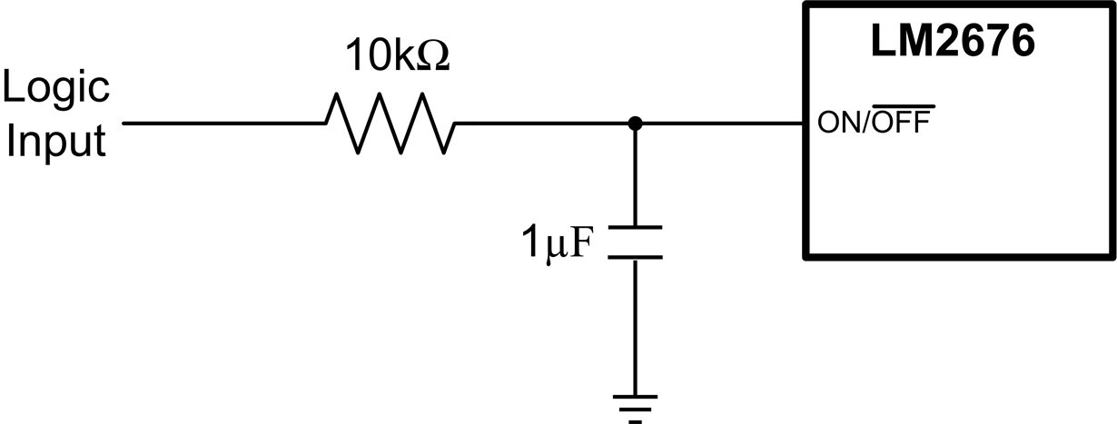
The above link describes voltage overshoot on output disable and the suggested solution. Would it be possible to see the electrical schematic for the enabling (On/Off) circuitry to better understand the efficiency of the suggested solution?

  • I have attached a schematic; the values can be adjusted.

  • Hi Frank,

    Thank you for your response.

    What I had in mind was to see the schematic of what is inside of the ON/OFF circuitry.

    The reason why, is  I thought that the ON/OFF acting on a threshold voltage (based on the LM2670 specs) and introducing RC circuit on its input will just cause a delay, but will not affect the over-voltage spike. But if the ON/OFF circuitry is affecting the duty cycle in the switcher, gradually reducing the energy stored in the inductance, the RC circuit on the input would prevent the over-voltage. 

    From the block diagram of LM2670 no conclusion can be made in regards to the above. That is why I would like to see the details.

    Best Regards,

    Michael

  • I can not share the deails of the internal circuits.

    However, I can say that the device has a sensitivity to the slew rate on the EN input that can

    cause the logic to not function correctly. 

    Also, any negative ring on the EN input, caused by long lnes and tast edges can create

    errors in the internanl logic.

    The RC filter helps to slow down any fast edges.