This thread has been locked.

If you have a related question, please click the "Ask a related question" button in the top right corner. The newly created question will be automatically linked to this question.

BQ51003: BQ51003 PCB design problem

Part Number: BQ51003
Other Parts Discussed in Thread: TIDA-00318

Hello,

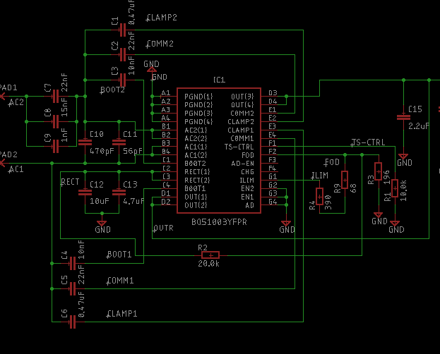
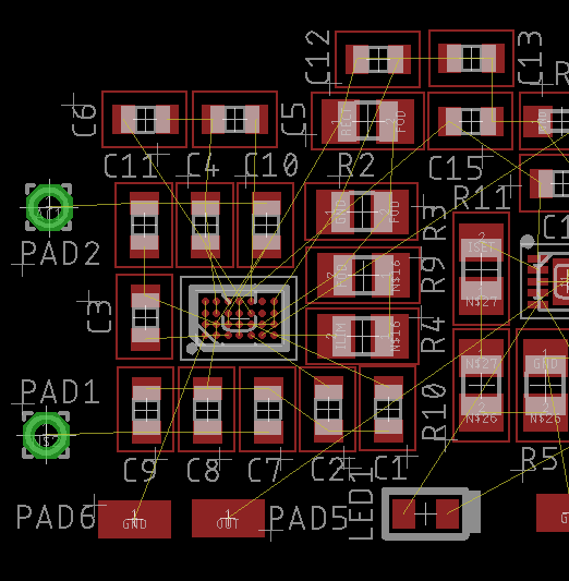
I am designing a PCB for wireless charger using BQ51003. I am facing problem in pulling out the signals from AC, CLAMP and FOD pins, as they are in the inner portion of IC.

Can anyone please suggest a way to do it?

Thank you in advance.

Best Regards,

Srujana Patel.

  • Take a look at TIDA-00318
    www.ti.com/.../TIDA-00318
    This is a design with bq51003 and the design files and gerber files are available for download.
  •  Hello Mr. Johns,

    Thank you for the response. I am facing issue with BGA package. And I couldn't find any solution in the TIDA-00318 designs.

    As you can see in the attached image, I used a capacitance of 10uF and 4.7uF at RECT and 2.2uF at OUT. I considered these values following the schematics document that is given in project design files in TI website.  I expect an output of 400mA at the Receiver end. But, the values that mentioned in the specifications document are completely different. I want to confirm if I can expect an output of 400mA at this receiver end. Please check the values given in the attached image.

    Also, the RECT and OUT bypass capacitors are at a distance as displayed in the second image. Would this anyway affect my output? Here, C12, C13 are my RECT capacitors and C15 is the OUT bypass capacitor.

    Thank you in advance.

    Best Regards,

    Srujana Patel.