This thread has been locked.

If you have a related question, please click the "Ask a related question" button in the top right corner. The newly created question will be automatically linked to this question.

WEBENCH® Tools/TPS5430: Layout development

Part Number: TPS5430

Tool/software: WEBENCH® Design Tools

Hello,

I'm developing a switched regulator using TPS5430 and I'd like to know which layout will preset better results.
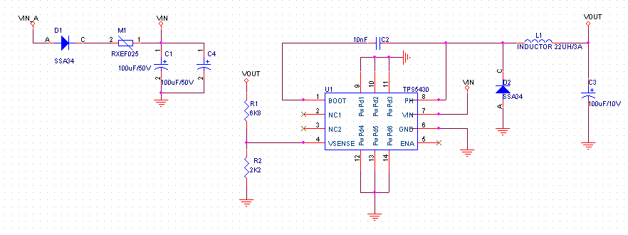
The circuit is:

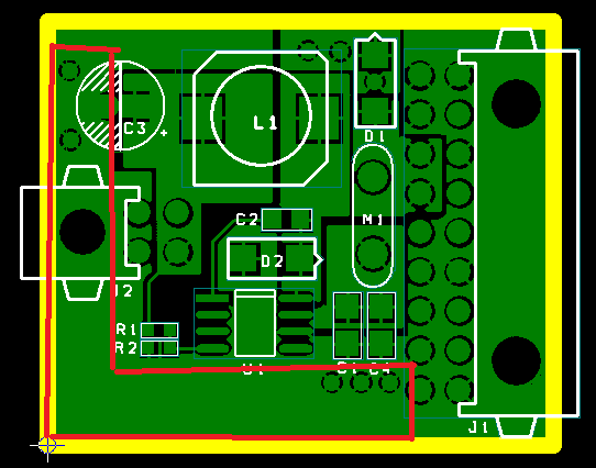
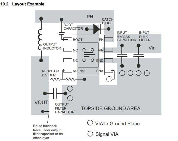
Datasheet recommends the following layout design:

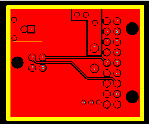
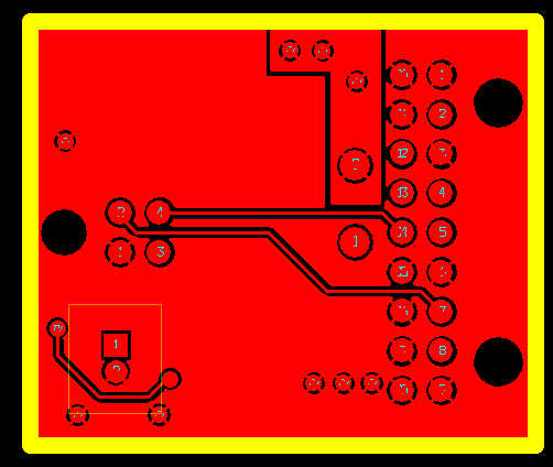
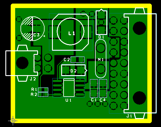
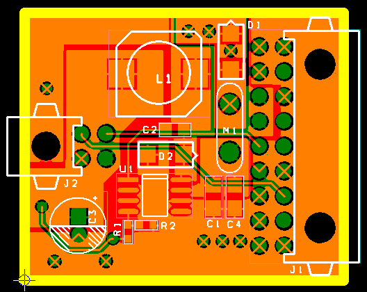
I designed 2 different layouts, changing the Cout position, but I don't kno which one would be better:

1.

2.

I can't change the board size and the J1 and J2 connectors need to be at this current position.

I'm in doubt about the following recommendantion regading the OUT loop: 

"It is important to keep the loop formed by the PH pin, Lout, Cout and GND as small as is practical."

Can anyboy enlight it for me?

  • There are two primary circulating current loops, the input from VIN pin to CIN + to Cin - to GND and the output loop from PH to Lout, Lout to Cout + and Cout - back to the GND pin. These are the loops you want to minimize as the carry large ac ripple currents. Neither of those layout look particularly appealing. Is the bottom side a dedicated GND plane? If so I would go with number 1 above. You may find you need some back side GND anyway for thermal performance.

  • Hi John!

    Thanks for your reply!

    Yes, in both cases there's a ground plane in the bottom side of the PCI, as shown below:

    1.

    2.

    Regarding the first loop, is there something that could improve the the layout? I follow the layout reccomendations, placing the input capacitors close to the Vin PIN, and putting a ground plane right above the capacitors (refer to the image where there's the topside ground area).

    D1 and M1 components are for protection purposes, so I used couper areas to connect them.

    As to the second loop, I'm in doubt regarding the first layout because of the ground area: according to the layout example, it reccomends to use the same ground "area" used in above the IC, and in this case the ground is connect from the up side of the PCB to the under part

    Or this is not a problem? That's why I routed the option 2, placing the capacitor so that I could use the "same" ground plane, but in this option (2), the loop from L1 - Vout - Cout is bigger.

    Regarding the resistor feedback to Vout, is there a specific recommendation to route this line?

    Thanks and best regards!