This thread has been locked.

If you have a related question, please click the "Ask a related question" button in the top right corner. The newly created question will be automatically linked to this question.

TPS65131-Q1: Used WEBENCH for the design. I get no output from either VPOS or VNEG.

Part Number: TPS65131-Q1
Other Parts Discussed in Thread: CSD25402Q3A

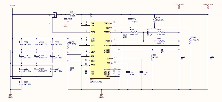
I am using the TI TPS65131-Q1 Buck/Boost Inverting supply. I ran through the TI WEBENCH to configure the circuit for 3.3V input and +/-5.0V output. I laid out my circuit exactly as the WeBench circuit. I even used the exact parts specified by WEBENCH.  I have checked that all of the parts are in correctly. I just get nothing on either the Vpos or the Vneg. This is the first time I have used one of the buck/boost supplies. It is completely different than a standard switcher. I am having a bit of trouble understanding what I should be seeing at different nodes to be able to debug the circuit. 

I attached a pdf of what I got from WEBENCH as well as my schematic.

Webench +5.0, -5.0 Supply using TPS65131-Q1.pdf

  • Hello Mark7389,

    Is it possible that you are using an N-channel MOSFET for Q1? This should be a P-channel MOSFET. For test purposes, you could just short this FET and check if then the boost converter is functional.

    As there are noise sensitive nodes as well as high power nodes on this part, I would encourage you to have a look at the EVM as reference for the layout. Sensitive nodes are CP and CN, FBx and VREF.

    The INP and OUTN nodes are the switch nodes of the 2 converters, so here you should see rectangular switching activity. In addition, please check what is happening during startup of the 3.3V.

    Best regards,
    Brigitte
  • Brigitte,

    I am indeed using a P-Channel MOSFET. The TI PN is CSD25402Q3A. I just noticed the symbol on the schematic is for an N-Channel. I started with a library part for the N-Channel to create the P-Channel and must have placed it before changing the sch symbol. I will try shorting across the part tomorrow to test for operation.

    The layout is based on the suggested layout from the datasheet as well as the EVM. I always try to follow as closely as possible.

    I will check the INP and OUTN for activity. Up to this point I have seen no activity on any of the pins. Either 3.3V or 0V steady on all pins. I will take a look at 3.3V during startup as well. I will check these first thing in the morning.

    Thank you,

    Mark
  • Brigitte,

    Near the TPS65131-Q1 the 3.3V input voltage has noise of 100-300mV at a frequency of around 1.32-1.35 MHz. This noise goes away the further you get the the device. Two inches away the 3.3V has about 20mV noise with no discernable frequency. I went through the circuit and checked the voltages at all of the pins on the device. Those reading are listed below.

    MOSFET (CSD25402Q3A)
    S - 3.3V
    D - 3.3V
    G - 0V with same switching noise seen on 3.3V

    TPS65131-Q1
    1, 24 (INP) - 3.3V
    4 (VIN) - 3.3V
    5, 6 (INN) - 3.3V
    7 (BSW) - 0V
    8 (ENP) - 3.3V
    10 (ENN) - 3.3V
    13, 14 (OUTN) - 60mV with 300mV Spikes at ~1.35MHz
    15 (VNEG) - 60mV
    16 (FBN) - 1.02V
    17 (VREF) - 1.26V
    18 (CN) - 660mV
    21 (CP) - 640mV
    22 (FBP) - 840mV
    23 (VPOS) - 3.3V

    VREF should be 1.213V (typ). FBP should be 1.213V as well and FBN should be 0V. all of these are off by quite a bit from what they should be. I have not checked the resistor values provided by WEBENCH. That will be my next step.

    Regards,

    Mark
  • Brigitte,

    One other comment/question I had is that the datasheet calls out a 4.7uF electrolytic capacitor on the INN input. The WEBENCH design instead called out (10) 0.47uF electrolytic caps. Trying to place 10 caps close to the device was next to impossible. I ended up placing one close, similar to the EVM and the other nine as close as I could. Could I swap out the one close 0.47uF cap for a 4.7uF cap for better noise immunity. I'm thinking this may be why all of the switching noise is surrounding this device. The datasheet also says that either an electrolytic or a ceramic cap may be used. If the electrolytic is used a 0.1uF ceramic must be place in parallel. Is that truly the case?

    Regards,

    Mark
  • Hello Mark,

    Normally ceramic capacitors should be used for this part. I need to check why you got 10 electrolytic ones with 470nF instead of one 4.7uF cap.

    Please check the design with one 4.7uF cap. In addition if you do not want to post your layout here, please send it to display_power_evm@list.ti.com with a reference to this thread.

    Best regards,
    Brigitte
  • Brigitte,

    I didn't have a 4.7uF that would fit in that location so I went with a 10uF. The noise spikes were slightly lower amplitude and the voltages in the list above were slightly different but no big changes.

    I will send you the layout via the email address you sent.

    Regards,

    Mark
  • Hello Mark,

    Thank you very much for the layout. Would you please send the GND layer as well?

    In a power supply GND is not just a reference voltage, but as well a power plane which is seeing a lot of current. Therefore it is important to have a very accurate knowledge about the current flow and make sure that noise cannot couple into the analog GND. I could imagine that the noise level on the GND is the issue with this design.

    Please have a very detailed look at the AGND layout of the EVM.

    It would be very good if we could check one converter at a time. Do you think you could disconnect the 2 ENx pins from the VIN signal and connect wires to ENN and ENP for enabling the converters separately?

    Best regards,
    Brigitte

  • Brigitte,

    I just sent you some additional files.

    I will take a look at the AGND layout of the EVM.

    Unfortunately I can't easily disconnect ENP and ENN to try them separately. I will take a look at the board again and see if there is any way  to separate them with out forever damaging the board. I only have 3 prototypes to work with so I need to be careful. I'll let you know if I can get something figured out.

    Regards,

    Mark

  • Brigitte,

    I see on the EVM how the AGND and PGND are designated in the schematic and then connected on the PCB. Unfortunately I followed the design provided by WEBENCH which had a single ground symbol for both AGND and PGND. In my haste to get this design done I did not pay enough attention to the EVM schematic and layout. At this point I'm not sure I can fix this on this rev of the board. I can easily fix it on the next rev but I would like to have the circuit working before I turn the board.

    Regards,

    Mark
  • Hello Mark,

    It seems that we both expect that this problem is resolved with the next layout revision. So I close this thread now. If it is not solved, either post a reply below or create a new thread.

    Best regards,
    Brigitte
  • Brigitte,

    That is my hope as well. I will use the EVM and compare to my circuit to see if I can get mine working on this board.

    I do have one more question. I am using the Q1 (Automotive) part as suggested by WEBENCH. Is there a difference in how this part works compared to the non-Q1 part?

    Mark

  • Hello Mark,

    The part is operating the same way as the commercial part.

    Best regards,
    Brigitte