This thread has been locked.

If you have a related question, please click the "Ask a related question" button in the top right corner. The newly created question will be automatically linked to this question.

BQ40Z50-R2: How Can I get bq40z50-R2 Cell Balancing Working?

Part Number: BQ40Z50-R2

Hi,

I got an issue regarding bq40z50-r2 cell blancing, I cannot get BQ40Z50-R2 cell balancing function, please help me to know how I can get it function.On circuit board, the original device is bq40z50-r1, later I programmed it with R2 version .srec file, the device is updated to r2.

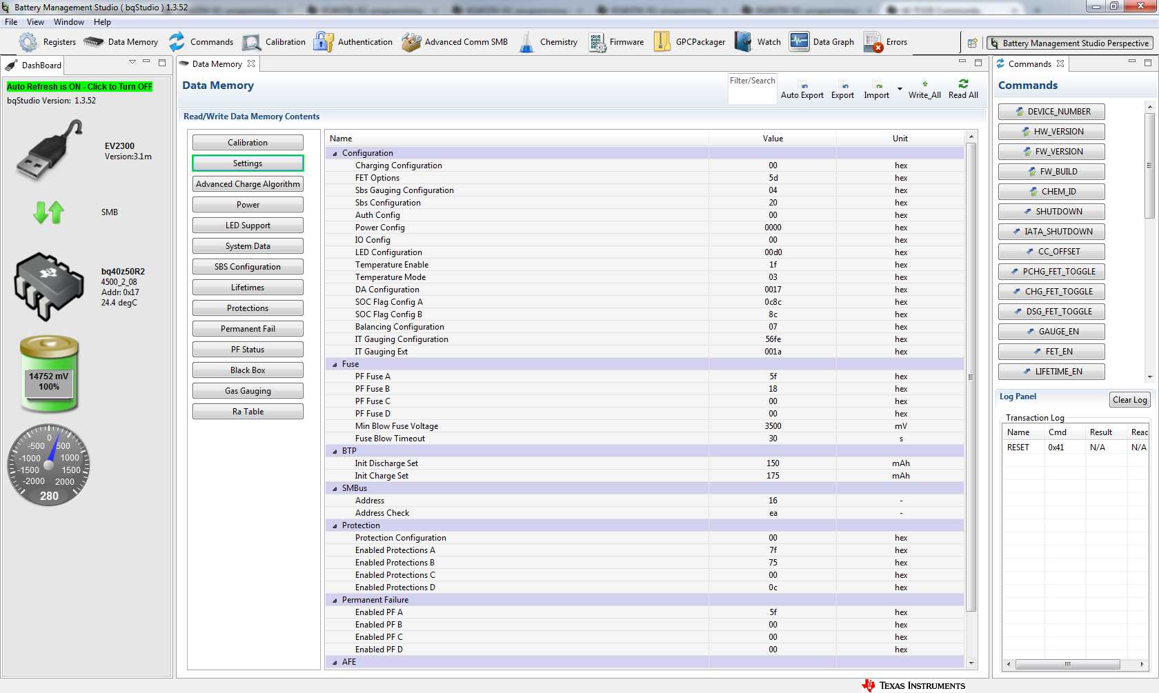
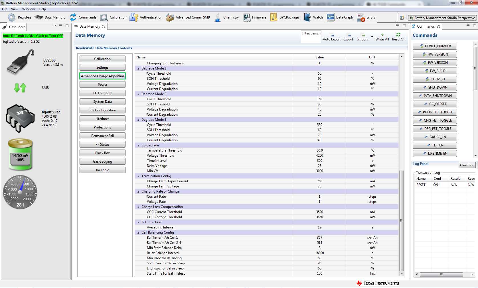
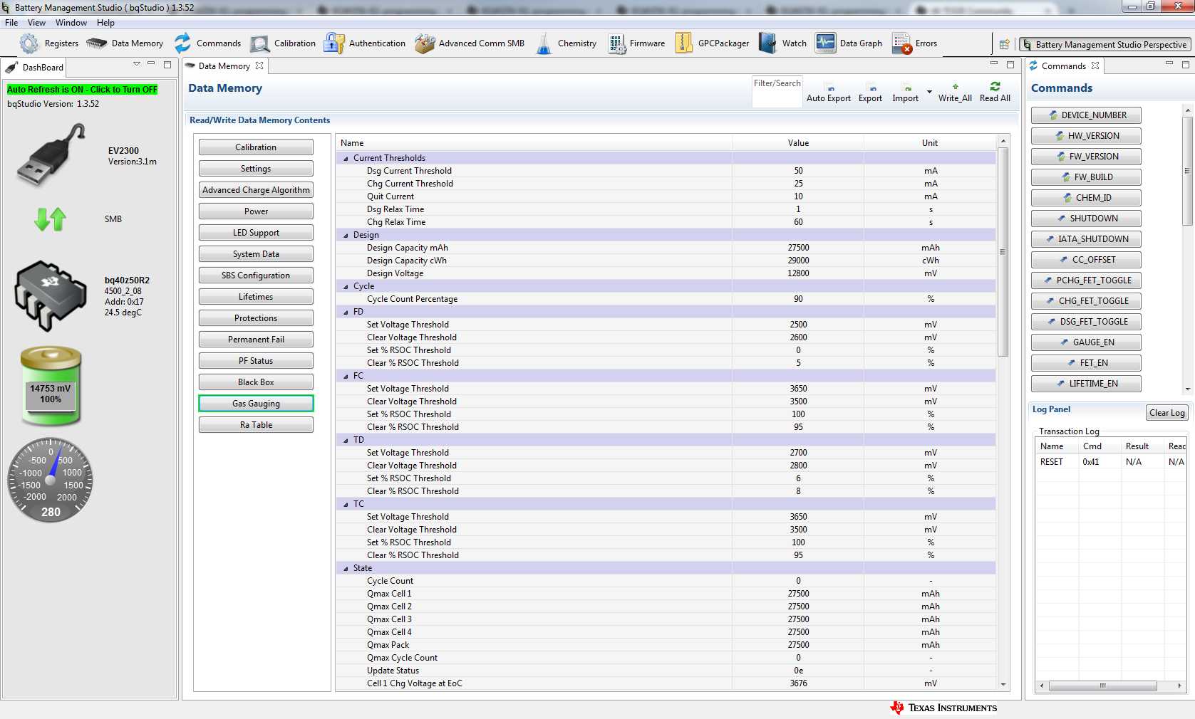
In my fuel gauge file, Balancing Configuration setting is 0x07, Cell Balancing Confi: Bal Time/mAh Cell1 is 367 s/mAh; Bal Time/mAh Cell 2-4 is 514 s/mAh; Min Start Balance Delta 3mv; Relax Balance Interval is 18000 s;Min Rsoc for Balancing is 80 %;Start RSOC for Bal in Sleep is 95 %;End Rsoc for Bal in Sleep is 60 %; StartTime for Bal in Sleep is 100 hrs. Update Status is 0x0e

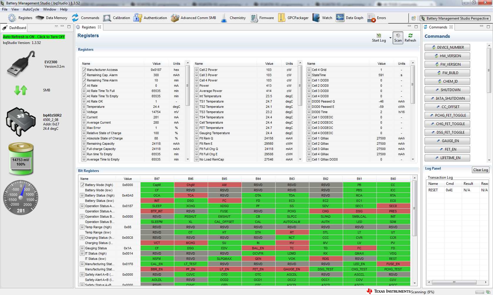
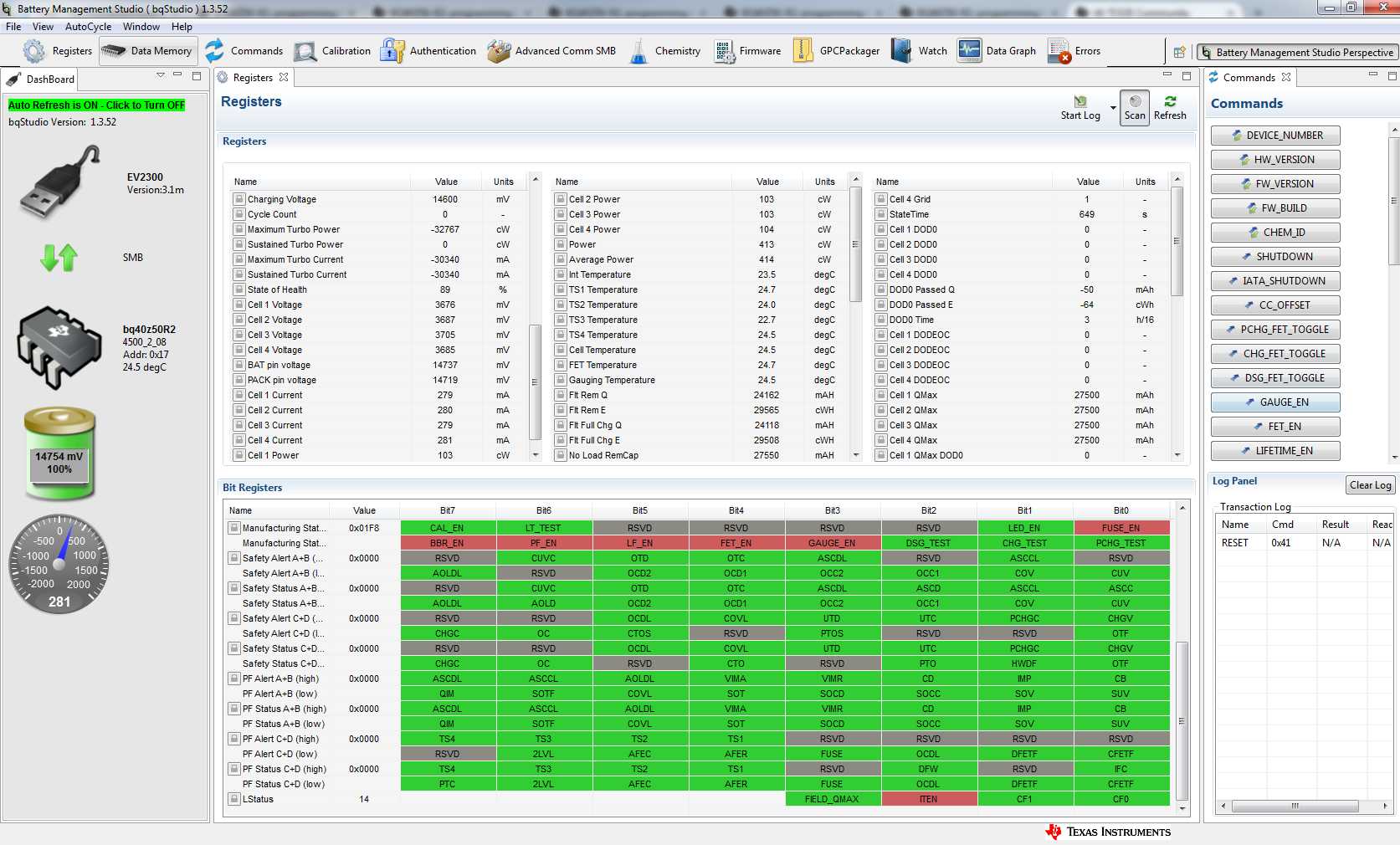
After power up the circuit board, RSOC reading is 100%, cell voltage are: cell1 3676mv, cell2 3686mv, cell3 3705mv, cell4 3684mv.

But no matter during a charging or a relax mode, under both of the conditions, I cannot get CB bit of Operation Status B set. I cannot see cell balancing working.

This is very urgent, my customer is waiting the circuit boards.

Please help me to know why cell balancing cannot work and how I should do to get it working.

Thank you very much!

Joy

  • Hi Joy,

    I have looped in the device expert and we will follow up with you tomorrow.

    Sincerely,
    Bryan Kahler
  • Hi Bryan,

    Thank you very much for your help, if you need any more info from me, please let me know.

    Thanks!

    Joy

    * Texas Instruments Data Flash File
    * File created Wed Nov 22 11:27:20 2017
    *
    * Device Number 4500
    * Firmware Version 2.08
    * Build Number 50
    * Order Number 0
    *
    * bqz Device Number 4500
    * bqz Firmware Version 2.08
    * bqz Build Number 50
    *
    * Field Order: Class name Subclass name Parameter name Parameter Value Display Units
    Calibration Voltage Cell Gain 12161 -
    Calibration Voltage Pack Gain 49387 -
    Calibration Voltage BAT Gain 49300 -
    Calibration Current CC Gain 1.923 mOhm
    Calibration Current Capacity Gain 1.923 mOhm
    Calibration Current Offset CC Offset 0 -
    Calibration Current Offset Coulomb Counter Offset Samples 64 -
    Calibration Current Offset Board Offset 0 -
    Calibration Current Offset CC Auto Config 7 hex
    Calibration Current Offset CC Auto Offset 7 -
    Calibration Temperature Internal Temp Offset 0.7 °C
    Calibration Temperature External1 Temp Offset -1.6 °C
    Calibration Temperature External2 Temp Offset 0.2 °C
    Calibration Temperature External3 Temp Offset 0.7 °C
    Calibration Temperature External4 Temp Offset 0.5 °C
    Calibration Internal Temp Model Int Gain -12143 -
    Calibration Internal Temp Model Int base offset 6232 -
    Calibration Internal Temp Model Int Minimum AD 0 -
    Calibration Internal Temp Model Int Maximum Temp 6232 0.1°K
    Calibration Cell Temperature Model Coeff a1 -11130 -
    Calibration Cell Temperature Model Coeff a2 19142 -
    Calibration Cell Temperature Model Coeff a3 -19262 -
    Calibration Cell Temperature Model Coeff a4 28203 -
    Calibration Cell Temperature Model Coeff a5 892 -
    Calibration Cell Temperature Model Coeff b1 328 -
    Calibration Cell Temperature Model Coeff b2 -605 -
    Calibration Cell Temperature Model Coeff b3 -2443 -
    Calibration Cell Temperature Model Coeff b4 4696 -
    Calibration Cell Temperature Model Rc0 11703 -
    Calibration Cell Temperature Model Adc0 11703 -
    Calibration Cell Temperature Model Rpad 0 -
    Calibration Cell Temperature Model Rint 0 -
    Calibration Fet Temperature Model Coeff a1 -11130 -
    Calibration Fet Temperature Model Coeff a2 19142 -
    Calibration Fet Temperature Model Coeff a3 -19262 -
    Calibration Fet Temperature Model Coeff a4 28203 -
    Calibration Fet Temperature Model Coeff a5 892 -
    Calibration Fet Temperature Model Coeff b1 328 -
    Calibration Fet Temperature Model Coeff b2 -605 -
    Calibration Fet Temperature Model Coeff b3 -2443 -
    Calibration Fet Temperature Model Coeff b4 4696 -
    Calibration Fet Temperature Model Rc0 11703 -
    Calibration Fet Temperature Model Adc0 11703 -
    Calibration Fet Temperature Model Rpad 0 -
    Calibration Fet Temperature Model Rint 0 -
    Calibration Current Deadband Deadband 3 mA
    Calibration Current Deadband Coulomb Counter Deadband 9 116nV
    Settings Configuration Charging Configuration 0 hex
    Settings Configuration FET Options 5d hex
    Settings Configuration Sbs Gauging Configuration 4 hex
    Settings Configuration Sbs Configuration 20 hex
    Settings Configuration Auth Config 0 hex
    Settings Configuration Power Config 0 hex
    Settings Configuration IO Config 0 hex
    Settings Configuration LED Configuration 00d0 hex
    Settings Configuration Temperature Enable 1f hex
    Settings Configuration Temperature Mode 3 hex
    Settings Configuration DA Configuration 17 hex
    Settings Configuration SOC Flag Config A 0c8c hex
    Settings Configuration SOC Flag Config B 8c hex
    Settings Configuration Balancing Configuration 7 hex
    Settings Configuration IT Gauging Configuration 56fe hex
    Settings Configuration IT Gauging Ext 001a hex
    Settings Fuse PF Fuse A 5f hex
    Settings Fuse PF Fuse B 18 hex
    Settings Fuse PF Fuse C 0 hex
    Settings Fuse PF Fuse D 0 hex
    Settings Fuse Min Blow Fuse Voltage 3500 mV
    Settings Fuse Fuse Blow Timeout 30 s
    Settings BTP Init Discharge Set 150 mAh
    Settings BTP Init Charge Set 175 mAh
    Settings SMBus Address 16 -
    Settings SMBus Address Check ea -
    Settings Protection Protection Configuration 0 hex
    Settings Protection Enabled Protections A 7f hex
    Settings Protection Enabled Protections B 75 hex
    Settings Protection Enabled Protections C 0 hex
    Settings Protection Enabled Protections D 0c hex
    Settings Permanent Failure Enabled PF A 5f hex
    Settings Permanent Failure Enabled PF B 0 hex
    Settings Permanent Failure Enabled PF C 0 hex
    Settings Permanent Failure Enabled PF D 0 hex
    Settings AFE AFE Protection Control 71 hex
    Settings AFE ZVCHG Exit Threshold 1500 mV
    Settings Manufacturing Mfg Status init 01f8 hex
    Advanced Charge Algorithm Temperature Ranges T1 Temp 0 °C
    Advanced Charge Algorithm Temperature Ranges T2 Temp 12 °C
    Advanced Charge Algorithm Temperature Ranges T5 Temp 20 °C
    Advanced Charge Algorithm Temperature Ranges T6 Temp 25 °C
    Advanced Charge Algorithm Temperature Ranges T3 Temp 30 °C
    Advanced Charge Algorithm Temperature Ranges T4 Temp 55 °C
    Advanced Charge Algorithm Temperature Ranges Hysteresis Temp 1 °C
    Advanced Charge Algorithm Low Temp Charging Voltage 3650 mV
    Advanced Charge Algorithm Low Temp Charging Current Low 10000 mA
    Advanced Charge Algorithm Low Temp Charging Current Med 10000 mA
    Advanced Charge Algorithm Low Temp Charging Current High 10000 mA
    Advanced Charge Algorithm Standard Temp Low Charging Voltage 3650 mV
    Advanced Charge Algorithm Standard Temp Low Charging Current Low 10000 mA
    Advanced Charge Algorithm Standard Temp Low Charging Current Med 10000 mA
    Advanced Charge Algorithm Standard Temp Low Charging Current High 10000 mA
    Advanced Charge Algorithm Standard Temp High Charging Voltage 3650 mV
    Advanced Charge Algorithm Standard Temp High Charging Current Low 10000 mA
    Advanced Charge Algorithm Standard Temp High Charging Current Med 10000 mA
    Advanced Charge Algorithm Standard Temp High Charging Current High 10000 mA
    Advanced Charge Algorithm High Temp Charging Voltage 3650 mV
    Advanced Charge Algorithm High Temp Charging Current Low 10000 mA
    Advanced Charge Algorithm High Temp Charging Current Med 10000 mA
    Advanced Charge Algorithm High Temp Charging Current High 10000 mA
    Advanced Charge Algorithm Rec Temp Charging Voltage 3650 mV
    Advanced Charge Algorithm Rec Temp Charging Current Low 10000 mA
    Advanced Charge Algorithm Rec Temp Charging Current Med 10000 mA
    Advanced Charge Algorithm Rec Temp Charging Current High 10000 mA
    Advanced Charge Algorithm Pre-Charging Current 88 mA
    Advanced Charge Algorithm Maintenance Charging Current 44 mA
    Advanced Charge Algorithm Voltage Range Precharge Start Voltage 2200 mV
    Advanced Charge Algorithm Voltage Range Charging Voltage Low 2500 mV
    Advanced Charge Algorithm Voltage Range Charging Voltage Med 3200 mV
    Advanced Charge Algorithm Voltage Range Charging Voltage High 3600 mV
    Advanced Charge Algorithm Voltage Range Charging Voltage Hysteresis 0 mV
    Advanced Charge Algorithm SoC Range Charging SoC Med 50 %
    Advanced Charge Algorithm SoC Range Charging SoC High 75 %
    Advanced Charge Algorithm SoC Range Charging SoC Hysteresis 1 %
    Advanced Charge Algorithm Degrade Mode 1 Cycle Threshold 50 -
    Advanced Charge Algorithm Degrade Mode 1 SOH Threshold 95 %
    Advanced Charge Algorithm Degrade Mode 1 Voltage Degradation 10 mV
    Advanced Charge Algorithm Degrade Mode 1 Current Degradation 10 %
    Advanced Charge Algorithm Degrade Mode 2 Cycle Threshold 150 -
    Advanced Charge Algorithm Degrade Mode 2 SOH Threshold 80 %
    Advanced Charge Algorithm Degrade Mode 2 Voltage Degradation 40 mV
    Advanced Charge Algorithm Degrade Mode 2 Current Degradation 20 %
    Advanced Charge Algorithm Degrade Mode 3 Cycle Threshold 350 -
    Advanced Charge Algorithm Degrade Mode 3 SOH Threshold 60 %
    Advanced Charge Algorithm Degrade Mode 3 Voltage Degradation 70 mV
    Advanced Charge Algorithm Degrade Mode 3 Current Degradation 40 %
    Advanced Charge Algorithm CS Degrade Temperature Threshold 50 °C
    Advanced Charge Algorithm CS Degrade Voltage Threshold 4200 mV
    Advanced Charge Algorithm CS Degrade Time Interval 300 s
    Advanced Charge Algorithm CS Degrade Delta Voltage 25 mV
    Advanced Charge Algorithm CS Degrade Min CV 3000 mV
    Advanced Charge Algorithm Termination Config Charge Term Taper Current 750 mA
    Advanced Charge Algorithm Termination Config Charge Term Voltage 75 mV
    Advanced Charge Algorithm Charging Rate of Change Current Rate 1 steps
    Advanced Charge Algorithm Charging Rate of Change Voltage Rate 1 steps
    Advanced Charge Algorithm Charge Loss Compensation CCC Current Threshold 3520 mA
    Advanced Charge Algorithm Charge Loss Compensation CCC Voltage Threshold 3650 mV
    Advanced Charge Algorithm IR Correction Averaging Interval 12 s
    Advanced Charge Algorithm Cell Balancing Config Bal Time/mAh Cell 1 367 s/mAh
    Advanced Charge Algorithm Cell Balancing Config Bal Time/mAh Cell 2-4 514 s/mAh
    Advanced Charge Algorithm Cell Balancing Config Min Start Balance Delta 3 mV
    Advanced Charge Algorithm Cell Balancing Config Relax Balance Interval 18000 s
    Advanced Charge Algorithm Cell Balancing Config Min Rsoc for Balancing 80 %
    Advanced Charge Algorithm Cell Balancing Config Start Rsoc for Bal in Sleep 95 %
    Advanced Charge Algorithm Cell Balancing Config End Rsoc for Bal in Sleep 60 %
    Advanced Charge Algorithm Cell Balancing Config Start Time for Bal in Sleep 100 hrs
    Power Power Valid Update Voltage 3500 mV
    Power Shutdown Shutdown Voltage 1750 mV
    Power Shutdown Shutdown Time 10 s
    Power Shutdown PF Shutdown Voltage 1750 mV
    Power Shutdown PF Shutdown Time 10 s
    Power Shutdown PS Shutdown Voltage 2500 mV
    Power Shutdown PS NoLoadResCap Threshold 0 mAh
    Power Shutdown Charger Present Threshold 3000 mV
    Power Shutdown Valid Wake up Comm Check Delay 100 s
    Power Sleep Sleep Current 10 mA
    Power Sleep Bus Timeout 5 s
    Power Sleep Voltage Time 5 s
    Power Sleep Current Time 20 s
    Power Sleep Wake Comparator 0 hex
    Power Ship FET Off Time 10 s
    Power Ship Delay 20 s
    Power Ship Auto Ship Time 1440 min
    Power Power Off Timeout 30 min
    Power Manual FET Control MFC Delay 60 0.25s
    Power IATA IATA Config 3 -
    Power IATA IATA Delay Time 10 s
    Power IATA IATA RSOC Threshold 30 %
    Power IATA IATA DeltaV Threshold 50 mV
    Power IATA IATA Delta RSOC 3 %
    Power IATA IATA Wake AbsRsoc 10 %
    Power IATA IATA Min Temperature 10 °C
    Power IATA IATA Max Temperature 40 °C
    Power IATA IATA Min Voltage 3000 mV
    Power IATA IATA Max Voltage 3650 mV
    Power IATA STORE IATA RM mAh 0 mAh
    Power IATA STORE IATA RM cWh 0 cWh
    Power IATA STORE IATA FCC mAh 0 mAh
    Power IATA STORE IATA FCC cWh 0 cWh
    Power IATA STORE IATA Flag 0 -
    Power Unintended Wakeup Delay 2 s
    Power Unintended Wakeup Count 3 -
    LED Support LED Config LED Flash Period 512 488us
    LED Support LED Config LED Blink Period 1024 488us
    LED Support LED Config LED Delay 100 488us
    LED Support LED Config LED Hold Time 4 s
    LED Support LED Config LED FC Time 60 mins
    LED Support LED Config CHG Flash Alarm 10 %
    LED Support LED Config CHG Thresh 1 0 %
    LED Support LED Config CHG Thresh 2 20 %
    LED Support LED Config CHG Thresh 3 40 %
    LED Support LED Config CHG Thresh 4 60 %
    LED Support LED Config CHG Thresh 5 80 %
    LED Support LED Config DSG Flash Alarm 10 %
    LED Support LED Config DSG Thresh 1 0 %
    LED Support LED Config DSG Thresh 2 20 %
    LED Support LED Config DSG Thresh 3 40 %
    LED Support LED Config DSG Thresh 4 60 %
    LED Support LED Config DSG Thresh 5 80 %
    System Data Manufacturer Data Manufacturer Info A Length 32 -
    System Data Manufacturer Data Manufacturer Info Block A01 61 Hex
    System Data Manufacturer Data Manufacturer Info Block A02 62 Hex
    System Data Manufacturer Data Manufacturer Info Block A03 63 Hex
    System Data Manufacturer Data Manufacturer Info Block A04 64 Hex
    System Data Manufacturer Data Manufacturer Info Block A05 65 Hex
    System Data Manufacturer Data Manufacturer Info Block A06 66 Hex
    System Data Manufacturer Data Manufacturer Info Block A07 67 Hex
    System Data Manufacturer Data Manufacturer Info Block A08 68 Hex
    System Data Manufacturer Data Manufacturer Info Block A09 69 Hex
    System Data Manufacturer Data Manufacturer Info Block A10 6a Hex
    System Data Manufacturer Data Manufacturer Info Block A11 6b Hex
    System Data Manufacturer Data Manufacturer Info Block A12 6c Hex
    System Data Manufacturer Data Manufacturer Info Block A13 6d Hex
    System Data Manufacturer Data Manufacturer Info Block A14 6e Hex
    System Data Manufacturer Data Manufacturer Info Block A15 6f Hex
    System Data Manufacturer Data Manufacturer Info Block A16 70 Hex
    System Data Manufacturer Data Manufacturer Info Block A17 71 Hex
    System Data Manufacturer Data Manufacturer Info Block A18 72 Hex
    System Data Manufacturer Data Manufacturer Info Block A19 73 Hex
    System Data Manufacturer Data Manufacturer Info Block A20 74 Hex
    System Data Manufacturer Data Manufacturer Info Block A21 75 Hex
    System Data Manufacturer Data Manufacturer Info Block A22 76 Hex
    System Data Manufacturer Data Manufacturer Info Block A23 77 Hex
    System Data Manufacturer Data Manufacturer Info Block A24 7a Hex
    System Data Manufacturer Data Manufacturer Info Block A25 78 Hex
    System Data Manufacturer Data Manufacturer Info Block A26 79 Hex
    System Data Manufacturer Data Manufacturer Info Block A27 30 Hex
    System Data Manufacturer Data Manufacturer Info Block A28 31 Hex
    System Data Manufacturer Data Manufacturer Info Block A29 32 Hex
    System Data Manufacturer Data Manufacturer Info Block A30 33 Hex
    System Data Manufacturer Data Manufacturer Info Block A31 34 Hex
    System Data Manufacturer Data Manufacturer Info Block A32 35 Hex
    System Data Manufacturer Info B Manufacturer Info Block B01 1 Hex
    System Data Manufacturer Info B Manufacturer Info Block B02 23 Hex
    System Data Manufacturer Info B Manufacturer Info Block B03 45 Hex
    System Data Manufacturer Info B Manufacturer Info Block B04 67 Hex
    System Data Integrity Static DF Signature 0 hex
    System Data Integrity Static Chem DF Signature 665a hex
    System Data Integrity All DF Signature 0 hex
    SBS Configuration Data Remaining AH Cap. Alarm 300 mAh
    SBS Configuration Data Remaining WH Cap. Alarm 432 cWh
    SBS Configuration Data Remaining Time Alarm 10 min
    SBS Configuration Data Initial Battery Mode 6000 hex
    SBS Configuration Data Specification Information 31 hex
    SBS Configuration Data Manufacture Date ######## date
    SBS Configuration Data Serial Number 1 hex
    SBS Configuration Data Manufacturer Name dc -
    SBS Configuration Data Device Name 5523773 -
    SBS Configuration Data Device Chemistry LION -
    Lifetimes Voltage Cell 1 Max Voltage 3430 mV
    Lifetimes Voltage Cell 2 Max Voltage 3460 mV
    Lifetimes Voltage Cell 3 Max Voltage 3429 mV
    Lifetimes Voltage Cell 4 Max Voltage 3446 mV
    Lifetimes Voltage Cell 1 Min Voltage 2795 mV
    Lifetimes Voltage Cell 2 Min Voltage 2921 mV
    Lifetimes Voltage Cell 3 Min Voltage 2892 mV
    Lifetimes Voltage Cell 4 Min Voltage 2884 mV
    Lifetimes Voltage Max Delta Cell Voltage 156 mV
    Lifetimes Current Max Charge Current 10380 mA
    Lifetimes Current Max Discharge Current -8672 mA
    Lifetimes Current Max Avg Dsg Current -7205 mA
    Lifetimes Current Max Avg Dsg Power -9298 cW
    Lifetimes Temperature Max Temp Cell 31 °C
    Lifetimes Temperature Min Temp Cell 18 °C
    Lifetimes Temperature Max Delta Cell Temp 6 °C
    Lifetimes Temperature Max Temp Int Sensor 34 °C
    Lifetimes Temperature Min Temp Int Sensor 17 °C
    Lifetimes Temperature Max Temp Fet 38 °C
    Lifetimes Safety Events No Of COV Events 0 events
    Lifetimes Safety Events Last COV Event 0 cycles
    Lifetimes Safety Events No Of CUV Events 0 events
    Lifetimes Safety Events Last CUV Event 0 cycles
    Lifetimes Safety Events No Of OCD1 Events 0 events
    Lifetimes Safety Events Last OCD1 Event 0 cycles
    Lifetimes Safety Events No Of OCD2 Events 0 events
    Lifetimes Safety Events Last OCD2 Event 0 cycles
    Lifetimes Safety Events No Of OCC1 Events 0 events
    Lifetimes Safety Events Last OCC1 Event 0 cycles
    Lifetimes Safety Events No Of OCC2 Events 0 events
    Lifetimes Safety Events Last OCC2 Event 0 cycles
    Lifetimes Safety Events No Of AOLD Events 0 events
    Lifetimes Safety Events Last AOLD Event 0 cycles
    Lifetimes Safety Events No Of ASCD Events 5 events
    Lifetimes Safety Events Last ASCD Event 0 cycles
    Lifetimes Safety Events No Of ASCC Events 0 events
    Lifetimes Safety Events Last ASCC Event 0 cycles
    Lifetimes Safety Events No Of OTC Events 0 events
    Lifetimes Safety Events Last OTC Event 0 cycles
    Lifetimes Safety Events No Of OTD Events 0 events
    Lifetimes Safety Events Last OTD Event 0 cycles
    Lifetimes Safety Events No Of OTF Events 0 events
    Lifetimes Safety Events Last OTF Event 0 cycles
    Lifetimes Charging Events No Valid Charge Term 0 events
    Lifetimes Charging Events Last Valid Charge Term 0 cycles
    Lifetimes Gauging Events No Of Qmax Updates 0 events
    Lifetimes Gauging Events Last Qmax Update 0 cycles
    Lifetimes Gauging Events No Of Ra Updates 6 events
    Lifetimes Gauging Events Last Ra Update 0 cycles
    Lifetimes Gauging Events No Of Ra Disable 7 events
    Lifetimes Gauging Events Last Ra Disable 0 cycles
    Lifetimes Power Events No Of Shutdowns 0 events
    Lifetimes Cell Balancing Cb Time Cell 1 0 h
    Lifetimes Cell Balancing Cb Time Cell 2 0 h
    Lifetimes Cell Balancing Cb Time Cell 3 2 h
    Lifetimes Cell Balancing Cb Time Cell 4 2 h
    Lifetimes Time Total Fw Runtime 164 h
    Lifetimes Time Time Spent In UT 0 h
    Lifetimes Time Time Spent In LT 0 h
    Lifetimes Time Time Spent In STL 76 h
    Lifetimes Time Time Spent In RT 70 h
    Lifetimes Time Time Spent In STH 12 h
    Lifetimes Time Time Spent In HT 0 h
    Lifetimes Time Time Spent In OT 0 h
    Protections CUV Threshold 2500 mV
    Protections CUV Delay 10 s
    Protections CUV Recovery 3000 mV
    Protections CUVC Threshold 0 mV
    Protections CUVC Delay 0 s
    Protections CUVC Recovery 0 mV
    Protections COV Threshold Low Temp 3750 mV
    Protections COV Threshold Standard Temp Low 3750 mV
    Protections COV Threshold Standard Temp High 3750 mV
    Protections COV Threshold High Temp 3750 mV
    Protections COV Threshold Rec Temp 3750 mV
    Protections COV Delay 10 s
    Protections COV Recovery Low Temp 3300 mV
    Protections COV Recovery Standard Temp Low 3300 mV
    Protections COV Recovery Standard Temp High 3300 mV
    Protections COV Recovery High Temp 3300 mV
    Protections COV Recovery Rec Temp 3300 mV
    Protections COV Latch Limit 0 -
    Protections COV Counter Dec Delay 10 s
    Protections COV Reset 15 s
    Protections OCC1 Threshold 11000 mA
    Protections OCC1 Delay 5 s
    Protections OCC2 Threshold 12000 mA
    Protections OCC2 Delay 2 s
    Protections OCC Recovery Threshold 50 mA
    Protections OCC Recovery Delay 8 s
    Protections OCD1 Threshold -11000 mA
    Protections OCD1 Delay 5 s
    Protections OCD2 Threshold -12000 mA
    Protections OCD2 Delay 2 s
    Protections OCD Recovery Threshold -50 mA
    Protections OCD Recovery Delay 8 s
    Protections OCD Latch Limit 0 -
    Protections OCD Counter Dec Delay 10 s
    Protections OCD Reset 15 s
    Protections AOLD Latch Limit 0 -
    Protections AOLD Counter Dec Delay 10 s
    Protections AOLD Recovery 5 s
    Protections AOLD Reset 15 s
    Protections AOLD Threshold 72 hex
    Protections ASCC Latch Limit 0 -
    Protections ASCC Counter Dec Delay 10 s
    Protections ASCC Recovery 5 s
    Protections ASCC Reset 15 s
    Protections ASCC Threshold 72 hex
    Protections ASCD Latch Limit 0 -
    Protections ASCD Counter Dec Delay 10 s
    Protections ASCD Recovery 5 s
    Protections ASCD Reset 15 s
    Protections ASCD Threshold 1 ff hex
    Protections ASCD Threshold 2 ff hex
    Protections OTC Threshold 55 °C
    Protections OTC Delay 2 s
    Protections OTC Recovery 50 °C
    Protections OTD Threshold 70 °C
    Protections OTD Delay 2 s
    Protections OTD Recovery 60 °C
    Protections OTF Threshold 80 °C
    Protections OTF Delay 2 s
    Protections OTF Recovery 65 °C
    Protections UTC Threshold 0 °C
    Protections UTC Delay 2 s
    Protections UTC Recovery 5 °C
    Protections UTD Threshold -25 °C
    Protections UTD Delay 2 s
    Protections UTD Recovery -15 °C
    Protections HWD Delay 10 s
    Protections PTO Charge Threshold 2000 mA
    Protections PTO Suspend Threshold 1800 mA
    Protections PTO Delay 1800 s
    Protections PTO Reset 2 mAh
    Protections CTO Charge Threshold 2500 mA
    Protections CTO Suspend Threshold 2000 mA
    Protections CTO Delay 54000 s
    Protections CTO Reset 2 mAh
    Protections OC Threshold 4500 mAh
    Protections OC Recovery 2 mAh
    Protections OC RSOC Recovery 90 %
    Protections CHGV Threshold 500 mV
    Protections CHGV Delay 30 s
    Protections CHGV Recovery -500 mV
    Protections CHGC Threshold 500 mA
    Protections CHGC Delay 2 s
    Protections CHGC Recovery Threshold 100 mA
    Protections CHGC Recovery Delay 2 s
    Protections PCHGC Threshold 50 mA
    Protections PCHGC Delay 2 s
    Protections PCHGC Recovery Threshold 10 mA
    Protections PCHGC Recovery Delay 2 s
    Permanent Fail SUV Threshold 2000 mV
    Permanent Fail SUV Delay 5 s
    Permanent Fail SOV Threshold 4500 mV
    Permanent Fail SOV Delay 5 s
    Permanent Fail SOCC Threshold 15000 mA
    Permanent Fail SOCC Delay 5 s
    Permanent Fail SOCD Threshold -15000 mA
    Permanent Fail SOCD Delay 5 s
    Permanent Fail SOT Threshold 85 °C
    Permanent Fail SOT Delay 5 s
    Permanent Fail SOTF Threshold 100 °C
    Permanent Fail SOTF Delay 5 s
    Permanent Fail Open Thermistor Threshold -50 °C
    Permanent Fail Open Thermistor Delay 5 s
    Permanent Fail Open Thermistor Fet Delta 20 °C
    Permanent Fail Open Thermistor Cell Delta 20 °C
    Permanent Fail QIM Delta Threshold 15 %
    Permanent Fail QIM Delay 2 updates
    Permanent Fail CB Max Threshold 240 h
    Permanent Fail CB Delta Threshold 40 h
    Permanent Fail CB Delay 2 cycles
    Permanent Fail VIMR Check Voltage 3500 mV
    Permanent Fail VIMR Check Current 10 mA
    Permanent Fail VIMR Delta Threshold 500 mV
    Permanent Fail VIMR Delta Delay 5 s
    Permanent Fail VIMR Duration 100 s
    Permanent Fail VIMA Check Voltage 3700 mV
    Permanent Fail VIMA Check Current 50 mA
    Permanent Fail VIMA Delta Threshold 200 mV
    Permanent Fail VIMA Delay 5 s
    Permanent Fail IMP Delta Threshold 300 %
    Permanent Fail IMP Max Threshold 400 %
    Permanent Fail IMP Ra Update Counts 2 Counts
    Permanent Fail CD Threshold 0 mAh
    Permanent Fail CD Delay 2 cycles
    Permanent Fail CFET OFF Threshold 5 mA
    Permanent Fail CFET OFF Delay 5 s
    Permanent Fail DFET OFF Threshold -5 mA
    Permanent Fail DFET OFF Delay 5 s
    Permanent Fail FUSE Threshold 5 mA
    Permanent Fail FUSE Delay 5 s
    Permanent Fail AFER Threshold 100 -
    Permanent Fail AFER Delay Period 2 s
    Permanent Fail AFER Compare Period 5 s
    Permanent Fail AFEC Threshold 100 -
    Permanent Fail AFEC Delay Period 5 s
    Permanent Fail 2LVL Delay 5 s
    PF Status Device Status Data Safety Alert A 0 hex
    PF Status Device Status Data Safety Status A 0 hex
    PF Status Device Status Data Safety Alert B 0 hex
    PF Status Device Status Data Safety Status B 0 hex
    PF Status Device Status Data Safety Alert C 0 hex
    PF Status Device Status Data Safety Status C 0 hex
    PF Status Device Status Data Safety Alert D 0 hex
    PF Status Device Status Data Safety Status D 0 hex
    PF Status Device Status Data PF Alert A 0 hex
    PF Status Device Status Data PF Status A 0 hex
    PF Status Device Status Data PF Alert B 0 hex
    PF Status Device Status Data PF Status B 0 hex
    PF Status Device Status Data PF Alert C 0 hex
    PF Status Device Status Data PF Status C 0 hex
    PF Status Device Status Data PF Alert D 0 hex
    PF Status Device Status Data PF Status D 0 hex
    PF Status Device Status Data Fuse Flag 0 hex
    PF Status Device Status Data Operation Status A 7181 hex
    PF Status Device Status Data Operation Status B 1000 hex
    PF Status Device Status Data Temp Range 10 hex
    PF Status Device Status Data Charging Status A 2 hex
    PF Status Device Status Data Charging Status B 0 hex
    PF Status Device Status Data Gauging Status 10 hex
    PF Status Device Status Data IT Status 1014 hex
    PF Status Device Voltage Data Cell 1 Voltage 3232 mV
    PF Status Device Voltage Data Cell 2 Voltage 3274 mV
    PF Status Device Voltage Data Cell 3 Voltage 3250 mV
    PF Status Device Voltage Data Cell 4 Voltage 3268 mV
    PF Status Device Voltage Data Battery Direct Voltage 13118 mV
    PF Status Device Voltage Data Pack Voltage 13241 mV
    PF Status Device Current Data Current 10228 mA
    PF Status Device Temperature Data Internal Temperature 25.6 °C
    PF Status Device Temperature Data External 1 Temperature 25.3 °C
    PF Status Device Temperature Data External 2 Temperature 24.8 °C
    PF Status Device Temperature Data External 3 Temperature 24.8 °C
    PF Status Device Temperature Data External 4 Temperature 25.2 °C
    PF Status Device Gauging Data Cell 1 Dod0 15420 -
    PF Status Device Gauging Data Cell 2 Dod0 15184 -
    PF Status Device Gauging Data Cell 3 Dod0 15258 -
    PF Status Device Gauging Data Cell 4 Dod0 15258 -
    PF Status Device Gauging Data Passed Charge -322 mAh
    PF Status AFE Regs AFE Interrupt Status 0 hex
    PF Status AFE Regs AFE FET Status 30 hex
    PF Status AFE Regs AFE RXIN 0 hex
    PF Status AFE Regs AFE Latch Status 0 hex
    PF Status AFE Regs AFE Interrupt Enable 10 hex
    PF Status AFE Regs AFE FET Control c0 hex
    PF Status AFE Regs AFE RXIEN 10 hex
    PF Status AFE Regs AFE RLOUT 7 hex
    PF Status AFE Regs AFE RHOUT 17 hex
    PF Status AFE Regs AFE RHINT 81 hex
    PF Status AFE Regs AFE Cell Balance 2 hex
    PF Status AFE Regs AFE AD/CC Control 19 hex
    PF Status AFE Regs AFE ADC Mux ef hex
    PF Status AFE Regs AFE LED Output 0 hex
    PF Status AFE Regs AFE State Control 40 hex
    PF Status AFE Regs AFE LED/Wake Control 32 hex
    PF Status AFE Regs AFE Protection Control 71 hex
    PF Status AFE Regs AFE OCD 77 hex
    PF Status AFE Regs AFE SCC ff hex
    PF Status AFE Regs AFE SCD1 ff hex
    PF Status AFE Regs AFE SCD2 ff hex
    Black Box Safety Status 1st Status Status A 0 hex
    Black Box Safety Status 1st Status Status B 0 hex
    Black Box Safety Status 1st Safety Status C 0 hex
    Black Box Safety Status 1st Safety Status D 0 hex
    Black Box Safety Status 1st Time to Next Event 0 s
    Black Box Safety Status 2nd Status Status A 0 hex
    Black Box Safety Status 2nd Status Status B 0 hex
    Black Box Safety Status 2nd Safety Status C 0 hex
    Black Box Safety Status 2nd Safety Status D 0 hex
    Black Box Safety Status 2nd Time to Next Event 0 s
    Black Box Safety Status 3rd Status Status A 0 hex
    Black Box Safety Status 3rd Status Status B 0 hex
    Black Box Safety Status 3rd Safety Status C 0 hex
    Black Box Safety Status 3rd Safety Status D 0 hex
    Black Box Safety Status 3rd Time to Next Event 255 s
    Black Box PF Status 1st PF Status A 4 hex
    Black Box PF Status 1st PF Status B 0 hex
    Black Box PF Status 1st PF Status C 0 hex
    Black Box PF Status 1st PF Status D 0 hex
    Black Box PF Status 1st Time to Next Event 255 s
    Black Box PF Status 2nd PF Status A 0 hex
    Black Box PF Status 2nd PF Status B 0 hex
    Black Box PF Status 2nd PF Status C 0 hex
    Black Box PF Status 2nd PF Status D 0 hex
    Black Box PF Status 2nd Time to Next Event 0 s
    Black Box PF Status 3rd PF Status A 0 hex
    Black Box PF Status 3rd PF Status B 0 hex
    Black Box PF Status 3rd PF Status C 0 hex
    Black Box PF Status 3rd PF Status D 0 hex
    Black Box PF Status 3rd Time to Next Event 0 s
    Gas Gauging Current Thresholds Dsg Current Threshold 50 mA
    Gas Gauging Current Thresholds Chg Current Threshold 25 mA
    Gas Gauging Current Thresholds Quit Current 10 mA
    Gas Gauging Current Thresholds Dsg Relax Time 1 s
    Gas Gauging Current Thresholds Chg Relax Time 60 s
    Gas Gauging Design Design Capacity mAh 27500 mAh
    Gas Gauging Design Design Capacity cWh 29000 cWh
    Gas Gauging Design Design Voltage 12800 mV
    Gas Gauging Cycle Cycle Count Percentage 90 %
    Gas Gauging FD Set Voltage Threshold 2500 mV
    Gas Gauging FD Clear Voltage Threshold 2600 mV
    Gas Gauging FD Set % RSOC Threshold 0 %
    Gas Gauging FD Clear % RSOC Threshold 5 %
    Gas Gauging FC Set Voltage Threshold 3650 mV
    Gas Gauging FC Clear Voltage Threshold 3500 mV
    Gas Gauging FC Set % RSOC Threshold 100 %
    Gas Gauging FC Clear % RSOC Threshold 95 %
    Gas Gauging TD Set Voltage Threshold 2700 mV
    Gas Gauging TD Clear Voltage Threshold 2800 mV
    Gas Gauging TD Set % RSOC Threshold 6 %
    Gas Gauging TD Clear % RSOC Threshold 8 %
    Gas Gauging TC Set Voltage Threshold 3650 mV
    Gas Gauging TC Clear Voltage Threshold 3500 mV
    Gas Gauging TC Set % RSOC Threshold 100 %
    Gas Gauging TC Clear % RSOC Threshold 95 %
    Gas Gauging State Cycle Count 0 -
    Gas Gauging State Qmax Cell 1 27500 mAh
    Gas Gauging State Qmax Cell 2 27500 mAh
    Gas Gauging State Qmax Cell 3 27500 mAh
    Gas Gauging State Qmax Cell 4 27500 mAh
    Gas Gauging State Qmax Pack 27500 mAh
    Gas Gauging State Qmax Cycle Count 0 -
    Gas Gauging State Update Status 6 -
    Gas Gauging State Cell 1 Chg Voltage at EoC 3650 mV
    Gas Gauging State Cell 2 Chg Voltage at EoC 3650 mV
    Gas Gauging State Cell 3 Chg Voltage at EoC 3650 mV
    Gas Gauging State Cell 4 Chg Voltage at EoC 3650 mV
    Gas Gauging State Current at EoC 250 mA
    Gas Gauging State Avg I Last Run -5244 mA
    Gas Gauging State Avg P Last Run -6709 cW
    Gas Gauging State Delta Voltage 4 mV
    Gas Gauging State Temp k 0.4 °C/256mW
    Gas Gauging State Temp a 12427 s
    Gas Gauging State Max Avg I Last Run -5904 mA
    Gas Gauging State Max Avg P Last Run -6838 cW
    Gas Gauging Turbo Cfg Min Turbo Power 0 cW
    Gas Gauging Turbo Cfg Ten Second Max C Rate -2 C
    Gas Gauging Turbo Cfg Ten Millisecond Max C Rate -4 C
    Gas Gauging Turbo Cfg High Frequency Resistance 15 mOhm
    Gas Gauging Turbo Cfg Reserve Energy % 0 %
    Gas Gauging Turbo Cfg Turbo Adjustment Factor 1 -
    Gas Gauging IT Cfg Load Select 7 -
    Gas Gauging IT Cfg Fast Scale Load Select 0 -
    Gas Gauging IT Cfg Load Mode 0 -
    Gas Gauging IT Cfg User Rate-mA 0 mA
    Gas Gauging IT Cfg User Rate-cW 0 cW
    Gas Gauging IT Cfg Reserve Cap-mAh 0 mAh
    Gas Gauging IT Cfg Reserve Cap-cWh 0 cWh
    Gas Gauging IT Cfg Predict Ambient Time 2000 s
    Gas Gauging IT Cfg Design Resistance 96 2^-10ohm
    Gas Gauging IT Cfg Pack Resistance 0 2^-10ohm
    Gas Gauging IT Cfg System Resistance 0 2^-10ohm
    Gas Gauging IT Cfg Ra Filter 80 %
    Gas Gauging IT Cfg Ra Max Delta 15 %
    Gas Gauging IT Cfg Reference Grid 4 -
    Gas Gauging IT Cfg Resistance Parameter Filter 65142 -
    Gas Gauging IT Cfg Near EDV Ra Param Filter 59220 -
    Gas Gauging IT Cfg Cell 1 Interconnect Resistance 0 2^-10ohm
    Gas Gauging IT Cfg Cell 2 Interconnect Resistance 0 2^-10ohm
    Gas Gauging IT Cfg Cell 3 Interconnect Resistance 0 2^-10ohm
    Gas Gauging IT Cfg Cell 4 Interconnect Resistance 0 2^-10ohm
    Gas Gauging IT Cfg Max Current Change % 10 %
    Gas Gauging IT Cfg Resistance Update Voltage 50 mV
    Gas Gauging IT Cfg Qmax Delta 5 %
    Gas Gauging IT Cfg Qmax Upper Bound 130 %
    Gas Gauging IT Cfg Term Voltage 10800 mV
    Gas Gauging IT Cfg Term V Hold Time 1 s
    Gas Gauging IT Cfg Term Voltage Delta 300 mV
    Gas Gauging IT Cfg Term Min Cell V 2800 mV
    Gas Gauging IT Cfg Max Simulation Iterations 30 -
    Gas Gauging IT Cfg Fast Scale Start SOC 10 %
    Gas Gauging IT Cfg Min Delta Voltage 0 mV
    Gas Gauging IT Cfg Max Delta Voltage 200 mV
    Gas Gauging IT Cfg DeltaV Max Voltage Delta 10 mV
    Gas Gauging Smoothing Smooth Relax Time 1000 s
    Gas Gauging Smoothing Term Smooth Start Cell V Delta 150 mV
    Gas Gauging Smoothing Term Smooth Final Cell V Delta 100 mV
    Gas Gauging Smoothing Term Smooth Time 20 s
    Gas Gauging Condition Flag Max Error Limit 100 %
    Gas Gauging Max Error Time Cycle Equivalent 24 h
    Gas Gauging Max Error Cycle Delta 0.05 %
    Gas Gauging SoH SoH Load Rate 5 Hr rate
    Ra Table R_a0 Cell0 R_a flag 555 -
    Ra Table R_a0 Cell0 R_a 0 758 2^-10ohm
    Ra Table R_a0 Cell0 R_a 1 35 2^-10ohm
    Ra Table R_a0 Cell0 R_a 2 44 2^-10ohm
    Ra Table R_a0 Cell0 R_a 3 58 2^-10ohm
    Ra Table R_a0 Cell0 R_a 4 34 2^-10ohm
    Ra Table R_a0 Cell0 R_a 5 44 2^-10ohm
    Ra Table R_a0 Cell0 R_a 6 44 2^-10ohm
    Ra Table R_a0 Cell0 R_a 7 47 2^-10ohm
    Ra Table R_a0 Cell0 R_a 8 41 2^-10ohm
    Ra Table R_a0 Cell0 R_a 9 41 2^-10ohm
    Ra Table R_a0 Cell0 R_a 10 78 2^-10ohm
    Ra Table R_a0 Cell0 R_a 11 80 2^-10ohm
    Ra Table R_a0 Cell0 R_a 12 96 2^-10ohm
    Ra Table R_a0 Cell0 R_a 13 129 2^-10ohm
    Ra Table R_a0 Cell0 R_a 14 187 2^-10ohm
    Ra Table R_a1 Cell1 R_a flag 555 -
    Ra Table R_a1 Cell1 R_a 0 741 2^-10ohm
    Ra Table R_a1 Cell1 R_a 1 34 2^-10ohm
    Ra Table R_a1 Cell1 R_a 2 43 2^-10ohm
    Ra Table R_a1 Cell1 R_a 3 47 2^-10ohm
    Ra Table R_a1 Cell1 R_a 4 27 2^-10ohm
    Ra Table R_a1 Cell1 R_a 5 35 2^-10ohm
    Ra Table R_a1 Cell1 R_a 6 35 2^-10ohm
    Ra Table R_a1 Cell1 R_a 7 37 2^-10ohm
    Ra Table R_a1 Cell1 R_a 8 33 2^-10ohm
    Ra Table R_a1 Cell1 R_a 9 33 2^-10ohm
    Ra Table R_a1 Cell1 R_a 10 63 2^-10ohm
    Ra Table R_a1 Cell1 R_a 11 65 2^-10ohm
    Ra Table R_a1 Cell1 R_a 12 78 2^-10ohm
    Ra Table R_a1 Cell1 R_a 13 104 2^-10ohm
    Ra Table R_a1 Cell1 R_a 14 151 2^-10ohm
    Ra Table R_a2 Cell2 R_a flag 555 -
    Ra Table R_a2 Cell2 R_a 0 758 2^-10ohm
    Ra Table R_a2 Cell2 R_a 1 35 2^-10ohm
    Ra Table R_a2 Cell2 R_a 2 44 2^-10ohm
    Ra Table R_a2 Cell2 R_a 3 48 2^-10ohm
    Ra Table R_a2 Cell2 R_a 4 28 2^-10ohm
    Ra Table R_a2 Cell2 R_a 5 36 2^-10ohm
    Ra Table R_a2 Cell2 R_a 6 36 2^-10ohm
    Ra Table R_a2 Cell2 R_a 7 39 2^-10ohm
    Ra Table R_a2 Cell2 R_a 8 34 2^-10ohm
    Ra Table R_a2 Cell2 R_a 9 34 2^-10ohm
    Ra Table R_a2 Cell2 R_a 10 65 2^-10ohm
    Ra Table R_a2 Cell2 R_a 11 66 2^-10ohm
    Ra Table R_a2 Cell2 R_a 12 79 2^-10ohm
    Ra Table R_a2 Cell2 R_a 13 107 2^-10ohm
    Ra Table R_a2 Cell2 R_a 14 155 2^-10ohm
    Ra Table R_a3 Cell3 R_a flag 555 -
    Ra Table R_a3 Cell3 R_a 0 741 2^-10ohm
    Ra Table R_a3 Cell3 R_a 1 34 2^-10ohm
    Ra Table R_a3 Cell3 R_a 2 43 2^-10ohm
    Ra Table R_a3 Cell3 R_a 3 47 2^-10ohm
    Ra Table R_a3 Cell3 R_a 4 27 2^-10ohm
    Ra Table R_a3 Cell3 R_a 5 35 2^-10ohm
    Ra Table R_a3 Cell3 R_a 6 35 2^-10ohm
    Ra Table R_a3 Cell3 R_a 7 37 2^-10ohm
    Ra Table R_a3 Cell3 R_a 8 33 2^-10ohm
    Ra Table R_a3 Cell3 R_a 9 33 2^-10ohm
    Ra Table R_a3 Cell3 R_a 10 63 2^-10ohm
    Ra Table R_a3 Cell3 R_a 11 65 2^-10ohm
    Ra Table R_a3 Cell3 R_a 12 78 2^-10ohm
    Ra Table R_a3 Cell3 R_a 13 104 2^-10ohm
    Ra Table R_a3 Cell3 R_a 14 151 2^-10ohm
    Ra Table R_a0x xCell0 R_a flag ffff -
    Ra Table R_a0x xCell0 R_a 0 896 2^-10ohm
    Ra Table R_a0x xCell0 R_a 1 41 2^-10ohm
    Ra Table R_a0x xCell0 R_a 2 52 2^-10ohm
    Ra Table R_a0x xCell0 R_a 3 69 2^-10ohm
    Ra Table R_a0x xCell0 R_a 4 40 2^-10ohm
    Ra Table R_a0x xCell0 R_a 5 52 2^-10ohm
    Ra Table R_a0x xCell0 R_a 6 52 2^-10ohm
    Ra Table R_a0x xCell0 R_a 7 55 2^-10ohm
    Ra Table R_a0x xCell0 R_a 8 48 2^-10ohm
    Ra Table R_a0x xCell0 R_a 9 48 2^-10ohm
    Ra Table R_a0x xCell0 R_a 10 92 2^-10ohm
    Ra Table R_a0x xCell0 R_a 11 95 2^-10ohm
    Ra Table R_a0x xCell0 R_a 12 114 2^-10ohm
    Ra Table R_a0x xCell0 R_a 13 152 2^-10ohm
    Ra Table R_a0x xCell0 R_a 14 221 2^-10ohm
    Ra Table R_a1x xCell1 R_a flag ffff -
    Ra Table R_a1x xCell1 R_a 0 896 2^-10ohm
    Ra Table R_a1x xCell1 R_a 1 41 2^-10ohm
    Ra Table R_a1x xCell1 R_a 2 52 2^-10ohm
    Ra Table R_a1x xCell1 R_a 3 69 2^-10ohm
    Ra Table R_a1x xCell1 R_a 4 40 2^-10ohm
    Ra Table R_a1x xCell1 R_a 5 52 2^-10ohm
    Ra Table R_a1x xCell1 R_a 6 52 2^-10ohm
    Ra Table R_a1x xCell1 R_a 7 55 2^-10ohm
    Ra Table R_a1x xCell1 R_a 8 48 2^-10ohm
    Ra Table R_a1x xCell1 R_a 9 48 2^-10ohm
    Ra Table R_a1x xCell1 R_a 10 92 2^-10ohm
    Ra Table R_a1x xCell1 R_a 11 95 2^-10ohm
    Ra Table R_a1x xCell1 R_a 12 114 2^-10ohm
    Ra Table R_a1x xCell1 R_a 13 152 2^-10ohm
    Ra Table R_a1x xCell1 R_a 14 221 2^-10ohm
    Ra Table R_a2x xCell2 R_a flag ffff -
    Ra Table R_a2x xCell2 R_a 0 896 2^-10ohm
    Ra Table R_a2x xCell2 R_a 1 41 2^-10ohm
    Ra Table R_a2x xCell2 R_a 2 52 2^-10ohm
    Ra Table R_a2x xCell2 R_a 3 69 2^-10ohm
    Ra Table R_a2x xCell2 R_a 4 40 2^-10ohm
    Ra Table R_a2x xCell2 R_a 5 52 2^-10ohm
    Ra Table R_a2x xCell2 R_a 6 52 2^-10ohm
    Ra Table R_a2x xCell2 R_a 7 55 2^-10ohm
    Ra Table R_a2x xCell2 R_a 8 48 2^-10ohm
    Ra Table R_a2x xCell2 R_a 9 48 2^-10ohm
    Ra Table R_a2x xCell2 R_a 10 92 2^-10ohm
    Ra Table R_a2x xCell2 R_a 11 95 2^-10ohm
    Ra Table R_a2x xCell2 R_a 12 114 2^-10ohm
    Ra Table R_a2x xCell2 R_a 13 152 2^-10ohm
    Ra Table R_a2x xCell2 R_a 14 221 2^-10ohm
    Ra Table R_a3x xCell3 R_a flag ffff -
    Ra Table R_a3x xCell3 R_a 0 896 2^-10ohm
    Ra Table R_a3x xCell3 R_a 1 41 2^-10ohm
    Ra Table R_a3x xCell3 R_a 2 52 2^-10ohm
    Ra Table R_a3x xCell3 R_a 3 69 2^-10ohm
    Ra Table R_a3x xCell3 R_a 4 40 2^-10ohm
    Ra Table R_a3x xCell3 R_a 5 52 2^-10ohm
    Ra Table R_a3x xCell3 R_a 6 52 2^-10ohm
    Ra Table R_a3x xCell3 R_a 7 55 2^-10ohm
    Ra Table R_a3x xCell3 R_a 8 48 2^-10ohm
    Ra Table R_a3x xCell3 R_a 9 48 2^-10ohm
    Ra Table R_a3x xCell3 R_a 10 92 2^-10ohm
    Ra Table R_a3x xCell3 R_a 11 95 2^-10ohm
    Ra Table R_a3x xCell3 R_a 12 114 2^-10ohm
    Ra Table R_a3x xCell3 R_a 13 152 2^-10ohm
    Ra Table R_a3x xCell3 R_a 14 221 2^-10ohm
  • More info, during I testing cell balance function, Update Status is 0x0e.

    Thanks,

    Joy

  • Hi Bryan,

    After I cycled my battery pack, I got bq40z50-r2 cell balance working now. And I found if I use the read out .srec file to program another circuit board, and if I use power supply and resistor divider to simulate battery cell, the bq40z50-r2 cannot start cell balancing. But if I connect the circuit board with real battery pack, the cell balancing can be working.

    I assue bq40z50-r2 FW is using the resistance of battery cell to be one of the condition to start cell balancing? Then in our circuit board testing department, we cannot test cell balance part circuit with resistor divider to simulate battery cell. Please confirm.

    Thanks,

    Joy