This thread has been locked.

If you have a related question, please click the "Ask a related question" button in the top right corner. The newly created question will be automatically linked to this question.

TPS62743: Power consumption issue - broken IC?

Expert 4650 points
Part Number: TPS62743

Dear e2e Community,

My customer is using our TPS62743YFPR on an end product already in production.

Few boards have a power consumption issue (1mA without load), while the voltage regulation seems to work well.

The 1mA measurement has been done with the ICs U2, U10 and F10 removed. An Agilent 34450A is used is series (>10Gohm input).

The application use a Lithium battery  (3V to 4.2V).

You will find below the screen shots performed with a lab source of 4V, instead of the battery.

As only few boards are concerned, we suspect our TPS to be defective and would like to understand what could damage it.

  • Does the oscillations, over shoot and under shoot on SW pin could damage the IC?
  • What is the max min transient voltage we can apply on SW pin?

SW signal on a defective board in Power Save Mode:

SW signal on a good board in PWM Mode with a 100mA load:

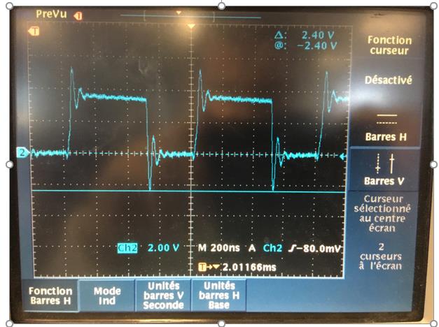
SW signal on a good board in Power Save Mode with a ~5µA load:

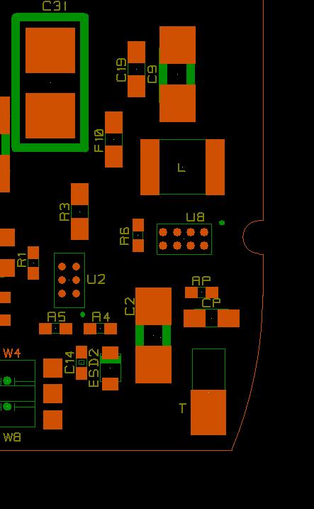
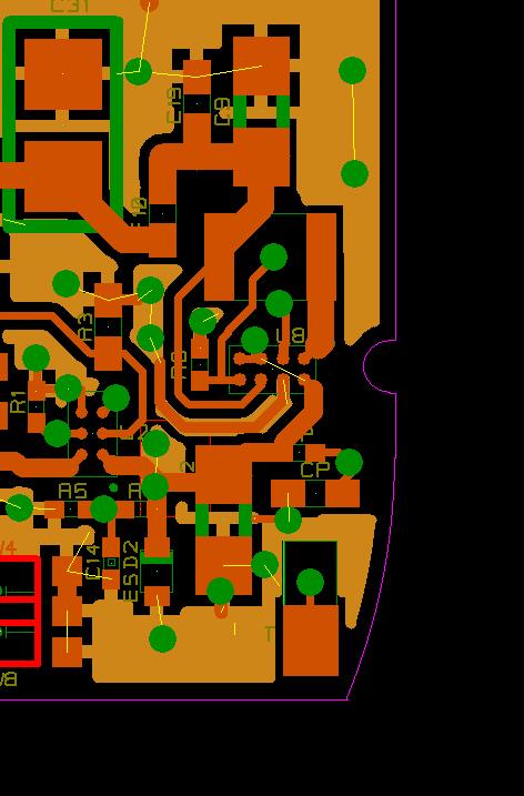
Here are the schematic and layout if it could help. Lout is a DFE201610C. Cout is a GRM188Z71A106MA73:

Regards,

  • Thanks for sharing many relevant details about the design.

    Can you share the raw measured values (Vin, Vout, Iin, Iout) for a passing and failing input current test? The first waveform shows a 2Vout, while the third waveform shows 3.3Vout. What do they have in their application?

    You can also remove a failing TPS62743, put it on an EVM, and see if the current consumption is still too high.

    The schematic looks ok, but the layout is not done perfectly. The input and output cap's GNDs are not connected directly to the GND pin. It looks like vias and a long trace are used.
  • Hello Chris,
    Thanks for your answers! :)
    Vin=3,9V ,Iout=5uA ( power safe mode)
    Endeed The third waveform shown 3.3V because vsel3/2/1="1"
    unfortunatly we cannot remove the failing TPS62743 and put in on an EVM We don't have the necessary equipment to weld it. ( too tiny)
    You're right Actually The input and output cap's GNDs are not connected directly to the GND pin. according to you this can deteriorate the SW pin waveform? or break the DC/DC ?
    I guess the ringing allow the output ( MOS &PMOS) to switch with bad timing so makes Overconsumption ?

    thanks!
  • Hi Yohann,

    Your CM that assembles the PCBs should be able to remove a failing device and install it on an EVM. We need to do this to make sure that it is the device which is not operating properly and not something else on the board.

    Have you replaced a failing device with a new device? Does that system now operate properly?