This thread has been locked.

If you have a related question, please click the "Ask a related question" button in the top right corner. The newly created question will be automatically linked to this question.

BQ76930: How to switch SHIP mode to Normal Mode

Part Number: BQ76930
Other Parts Discussed in Thread: TIDA-00792

Hi Guys

After from NORMAL Mode  switching to the SHIP Mode. Press the TS1 activation and write 0x00 at address 0 x04. But it can't go back to NORMAL Mode.The voltage data read from bq76930 is always wrong. I would like to ask how to return to NORMAL Mode, the NORMAL initial activation work status?

Thanks

  • Mr Vincent:
    To get the part of SLEEP into Active mode, the bq76930 requires an external "wake pulse" (>1V))on the TS1 Pin on the bottom group. The boot sequence and the voltage after the BOOT on TS1( >1V)--CAP1--> REGOUT--SCLK-->CAP2--CAP3.

    For the device to be commanded via the I2C into SLEEP mode by the controller; The device needs a 2 register write [SHUT_A, SHUT _B]= [0,1], [SHUT_A, SHUT _B]= [1,0]
  • Dear Vish,

    1. I am confused about Bq76930 TS1 pin~

    I have one BQ76930 EVM, everytime I power on, I need to push the TS1 boot button,Then REGOUT normally~I want to know if  the "wake pulse" (>1V))on the TS1 can be automatic。

    I have read the document "bq769x0 Boot Switch Alternatives" but still don't know how to design and the  theory~Need your help~

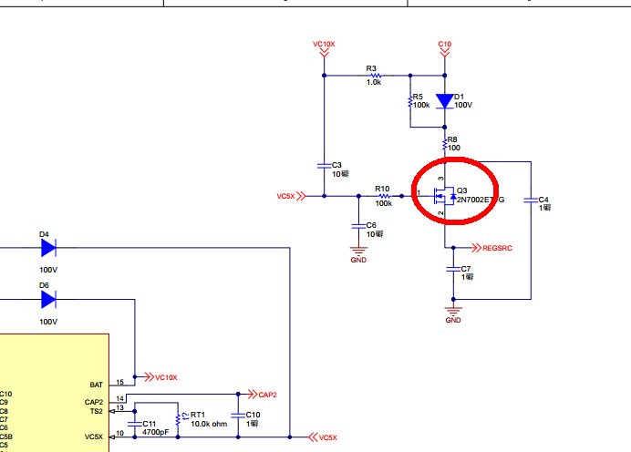
    2 I want to know the function of Q3? Why I need this FET?  Hope for your reply~

    .

  • Hi Fawn,
    Yes the TS1 pin requires a rising edge to wake up. If a signal is not available, a pulse circuit could be used triggered by some condition which can be applied. See the apnote you mentioned. Also see TIDA-00792 for a high side example.That design has a circuit triggered by a rise in PACK+ voltage and component patterns for an external signal. For circuit information you might consult your favorite texts, a colleague or search for design references on the web.

    Q3 in the schematic clip drops the voltage from the battery to the REGSRC pin to reduce the voltage and limit power in the bq76930. If C10 were 40V this would be too high for REGSRC pin. If 20 mA were drawn from the 40V battery to a 3.3V REGOUT total dissipation would be 0.734W. The transistor and resistor allow some of the dissipation to be outside the IC, size these components for the load current. Q3 operates as source follower configuration or common drain amplifier, you might search for those circuits.