This thread has been locked.

If you have a related question, please click the "Ask a related question" button in the top right corner. The newly created question will be automatically linked to this question.

LM3423: Unstable output current

Part Number: LM3423

Dear all,

I am using the LM3423 buck-boost evaluation board for testing a design. Ouput current goes unstable as Vin approaches the upper part of the range.

Vin: 7 V to 31 V
Vout: 10.5 V
Iout: 0.25 A
PWM is to be used for dimming

At input voltages at  around 24 V and below, everything works fine. Some overshoot at the start of each pulse, but we should be fine with that.
Se picture below. Voltage is measured over Rsns. 100 mV corresponds to the desired 0.25 A.

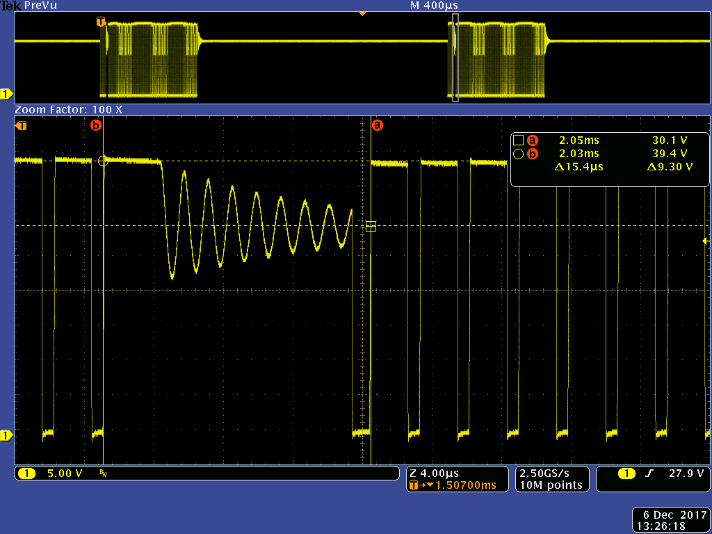
When input voltage goes above around 26 V, output current goes unstable. There is also audible noise from the inductor. 
See picture below (Vin = 30 V):

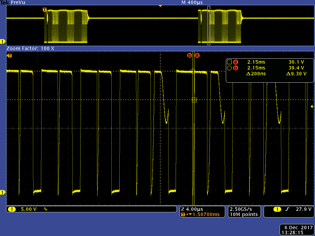
Next 2 pictures are from switching node, where it is obvious that pulses are skipped or differs much from estimated duty-cycle. Vin = 30 V. (When Vin = 24 V, all pulses have expected pulse width)

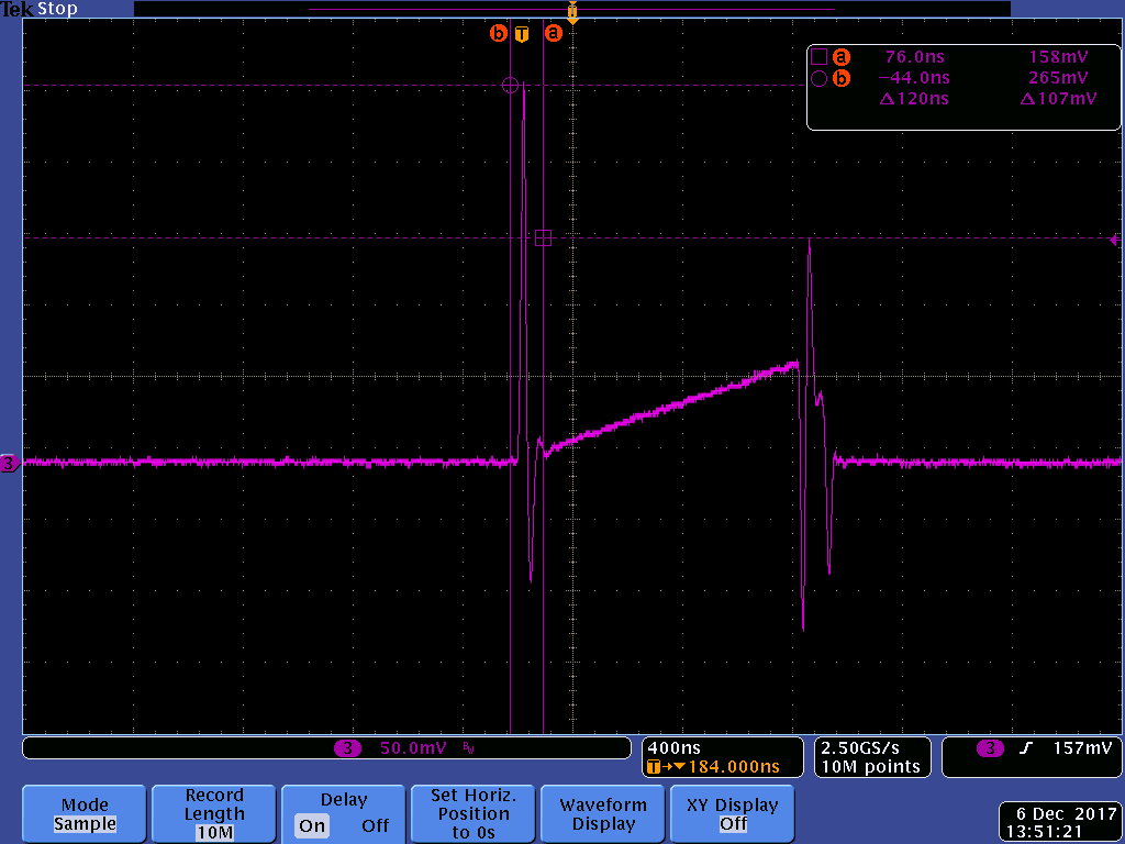
Perhaps it has something to do with that discontinuos mode is entered, so I measured the voltage over a 0.1 ohm resistor in series with the inductor, to see inductor current.
See picture below, I am not really sure what I see here, but seems current crosses 0 and discontinuous mode is entered but this is already at 24 V where things are OK. Unfortunately I do not have a current or differential probe... :

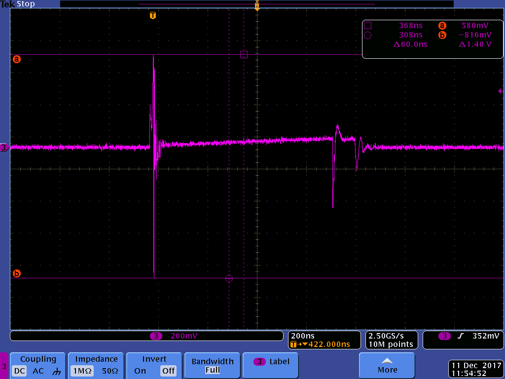
Another thing is that  I have been thinking of is if the Rlim sensing triggers on overcurrent. Below picture is from measuring over Rlim. There is a spike that goes above trigger voltage of 245 mV, but shouldn't this be ignored because of blanking circuit ?

I have tried changing these values and only see small changes in behavior:
- L = 47 uH, 33 uH, 68 uH 100 uH
- Ccomp = 100 nF 220nF, 470 nF, 1 uF, 2 uF.
- Chspn = 47nF, 100 nF 220 nF


Other observations:
- FLT is never triggered
- OVP is never triggered
- LRDY is triggered in those cases ILED swings above/below threshold

The design is from webbench and I checked it against design guidelines, making all calculations, and they align. See attached schematic.
The design is run on the LM3423 buck-boost eval board where I kept the FETs, diode and inductor from the original board. Otherwise board is update according to webbench design.

Do you have any ideas on how to get clean output current also as Vin approaches 30 V?
Please help me out this is frustrating...

  • Hello,

    We will get this figured out but it does kind of look like you are hitting current limit every other time the switch tries to turn on at higher voltages. Do you have a scope shot of IS at 30V input? It would also help to not have the bandwidth limiter on there, at least on the lowest setting (use 150MHz and not 20MHz). A differential probe would be good, but you can use a standard on and just remove the tip. Wrap wire around the ground ring and have a very short ground loop to measure directly across Rlim. That would give you a better idea.

    One thing I noticed that can cause issues is that the diode is way oversized for the application. This can cause problems due to excessive parasitics when you drive at a lower current. The first thing I would try is to replace it with something much smaller like a 60V or 100V, 1A schottky and see if that helps. It is often the noise generated by the diode recovery and parasitic capacitance that will trigger a current limit.

    You could also play with the value for R17 to speed/slow the switch turn on/off to reduce the spiking. That might help with the noise as well. But I would start with looking closely at IS and trying a more properly rated diode. Let me know if it helps or not.

    Regards,

    Clint

  • Hello Clint,

    thank you for your prompt response, it is very much appreciated! I did not get a chance to make measurements until today...

    It seems to do with current limit as you suggest!

    I first tried a 1 A diode (ES1D). Now output current looks clean. However, when I bypassed Q2, as in our design we would like to be without it for simplicity, then current is noisy over the full input voltage range....

    I changed diode to a 3A (MBR340T3G) and now  output is clean even when Q2 is bypassed!

    If I would like to  increase margin here, is there a way to filter the IS input e.g. with a RC-filter? ....or will perhaps phase margin  be affected?

    For final design, hopefully I will be able to optimize PCB layout and look for an even better diode with low capacitance and fast recovery, to get better margin.

    Below picture is IS pin with original 12CWQ010 diode. (BW=500 MHz), Vin = 30V

    Next picture (below) is with ES2D diode. Ringing is reduced, but peak-peak spikes are still substantial.

    Next picture (below) is with MBR340T3G diode. Now there is some more margin regarding peak-peak spikes.

  • Hello,

    One common way to reduce noise created by the diode is to put a ferrite bead in series with it.

    But you can also just use some filtering on IS, it will not affect the stability much if you use low values. I would try maybe a 10ohm resistor with a 1nF capacitor to start and then tweak it if needed.

    Regards,

    Clint

  • Very good! I will add those features to our design.

    Thank you for prompt responses to my questions!