This thread has been locked.

If you have a related question, please click the "Ask a related question" button in the top right corner. The newly created question will be automatically linked to this question.

TPS40200: Shutdown with small load. Slow recovery

Part Number: TPS40200
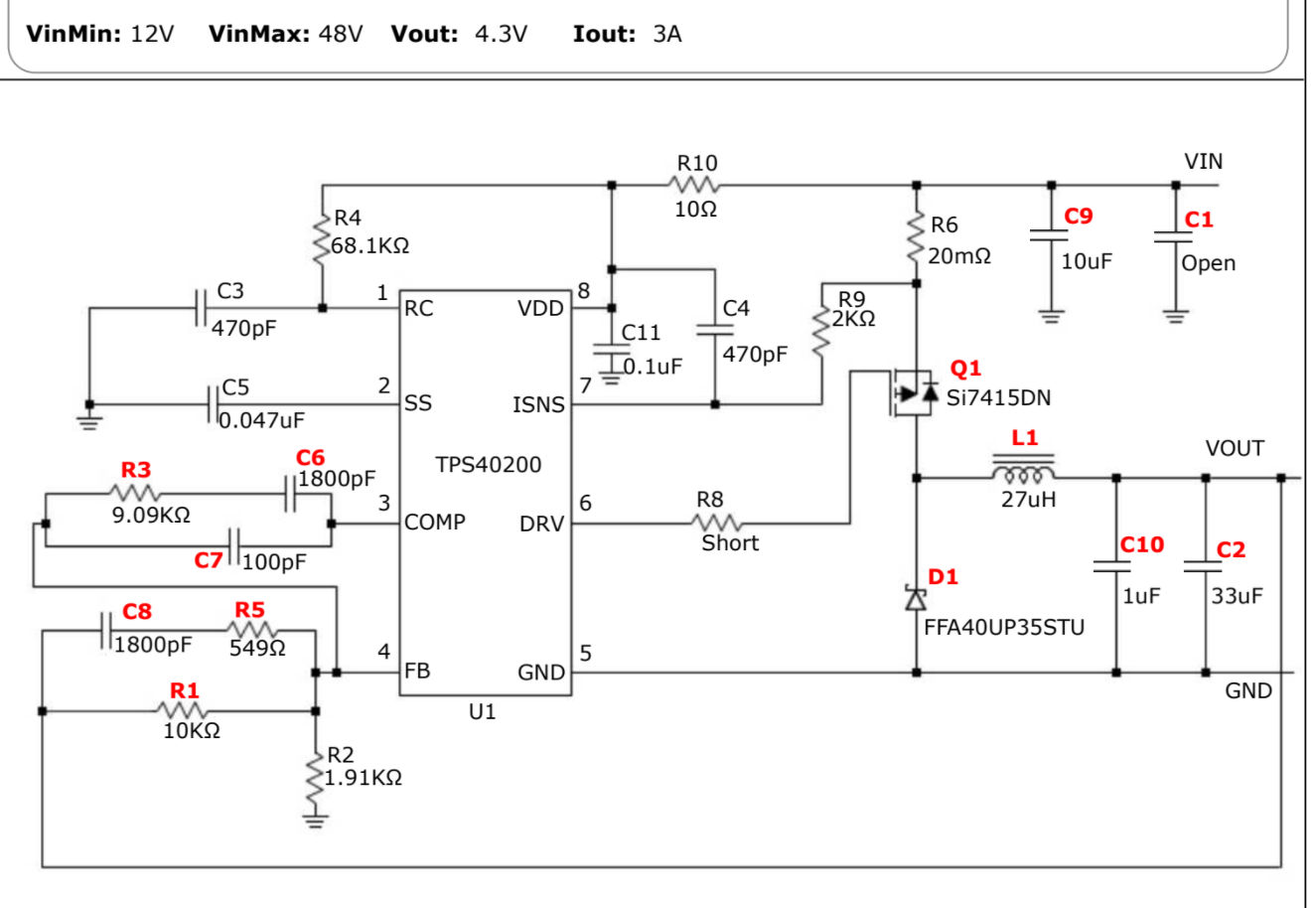
Other Parts Discussed in Thread: LM76003, TPS54360, TPS54560, LMR16030

Hi, I'm using TPS40200 on my design and while all components arrive, I've using some similar parts (+- 20%) to test. I dont expect to work perfectly but a little bit. The problem is I can't achieve this.

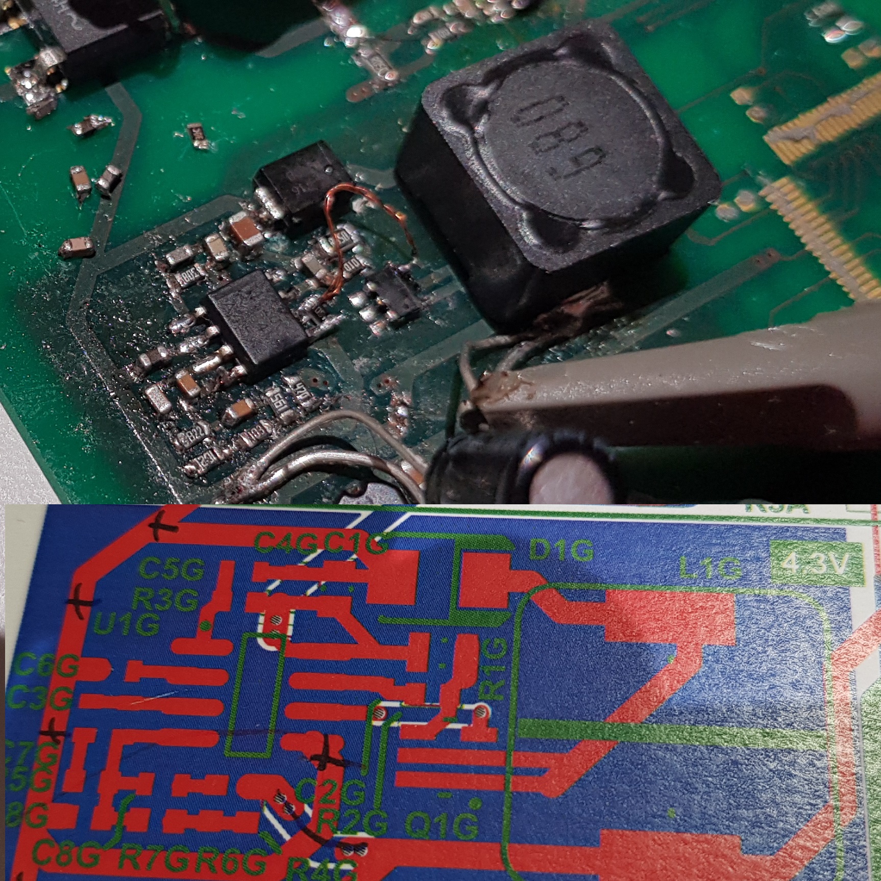
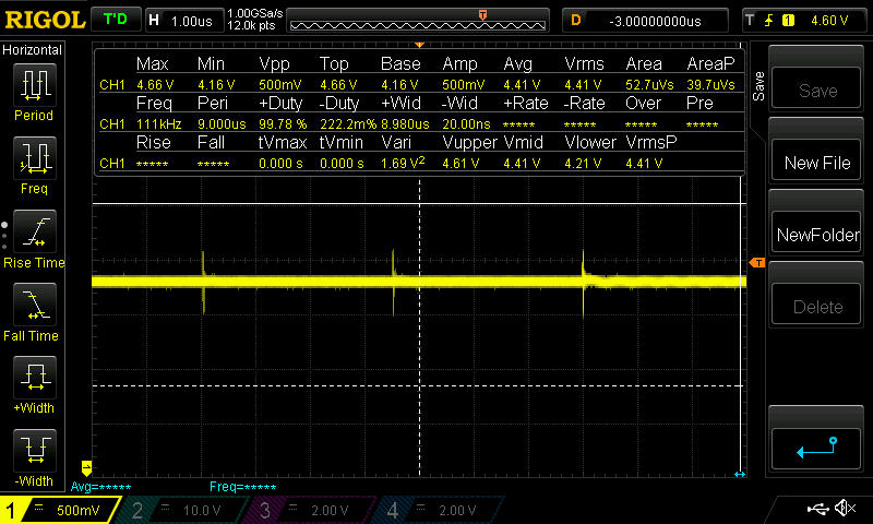
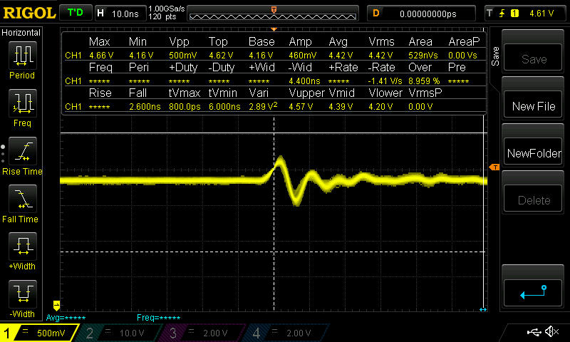
The voltage at the output is accurate but fall with more than 100mA. I've seen the signal (suposely square) at fet input has some damping (maybe bad layout) and with 1M resistor to ground there seems to hold more current at the output, but not too much.

I'm using 68uH inductor (CDRH127) and 33uF electrolitic capacitor at output. With 22uH (CD54) instead 68uH the current at the output is higher (arround 1A at 12Vin and 100mA with 30Vin) but when Vin goes up the supply goes down...

So I have two questions:

-Why TPS40200 is so extrict with components/layout when other DC/DC are not?

-What are the conditions fot TPS40200 to shutdown? (There is no Vin low here and I've increased the current with load so I think is not soft start related, there is not overcurrent...)

Thanks


  • You may need more output capacitors. You design is pretty similar to the typical design on page 19 of the datasheet. It has 100uF output capacitor.

    We can help debugging if you can provide more details. The waveforms of the VIN, Vout and switch node (where Q1 is tied to D1 and L1) should help to understand the operating status of the buck converter. Please provide waveforms in good condition and bad conditions.

    Layout in pdf should also help.

    Regards,

    Yang
  • 13vin, CDRH127 68uH inductor, CPH6354 fet, B360B diode, 33uF+1uF at output:

    Yellow Vout, Blue Vin:

    Blue Switch node (weird...)

    Blue, TPS40200 pin 6 

    With 100mA load the damping in switch node is dissapeared, only spikes left. with little bit more load (110mA for example) stops working (0V at output) and a square wafe of 6,5% on duty is on the switch node..

    This is the board. It is a prototype, not too clean, but I dont expected to work so bad :/ (the wire from TPS40200 pin 6 to the fet is in paralell with PCB wire (I wanted to test if was a wire impedance problem...)

  • All switching regulators are sensitive to layout, not just TPS40200. Since it is a controller, you have to layout the external FET and diode, it makes the layout more complicated. If the operation range you need is Vin=12V-48V, load = 3A max, as stated in the schematic above, you may consider a non-synchronous buck such as TPS54360, TPS54560, LMR16030 (non-sync regulator has high side FET integrated, you need power diode on the board), or you can consider a synchronous buck such as LM76003 (sync regulators have both high side and low side FET integrated). The PCB layout is easier with FET integrated.

    For the layout above, the key element is to keep the area enclosed by Vin cap (C9, C1), R6, Q1, D1 as small as possible. This loop and these components contains pulsing current, which generates more noise if the loop area is larger. I didn't find C9 on the layout, I think it is the two caps at the left hand side of D1. C1 shouldn't be open, it should be a 1uF high voltage cap for bypassing. When the ground trace goes from D1 around the IC to the IC ground, all the compensation and feedback components tied to this ground trace will pick up switching noise directly. The gate drive signal also contains pulsing signal, with much lower current though. It is not good to have it fly over as it is now.

    How many layer is your board? To verify the design, I'd suggest modify an EVM to your component values and check the behavior. If the BOM works on the EVM, then improve the layout to make it work on your board.

    Hope these helps.

    -Yang
  • I'm testing with EVM, changing the components with my design but I have switch noise even at no load, and much more at 2A, I think this noise is not secure (1.20Vpp). ¿any advice? I'm testing with some capacitors but no success.

    No load 1uS

    No load 10nS

    2A load 10ns 

  • I've changed the electrolytic output capacitor for tantalum and now the noise ripple at 2A is 400mV, much better but still need an improve
  • If you use a 10Ohm (or start with 5Ohm) resistor on R8 to slow down the gate drive voltage, the ringing will be lowered. You could also consider snubber circuit from SW node to ground. Please note how you probe the switch node make a big difference as well. Use as small as possible ground loop for the probe to reduce the noise coupled through the probing loop.