This thread has been locked.

If you have a related question, please click the "Ask a related question" button in the top right corner. The newly created question will be automatically linked to this question.

LM22678: Failures

Part Number: LM22678

Good Afternoon,
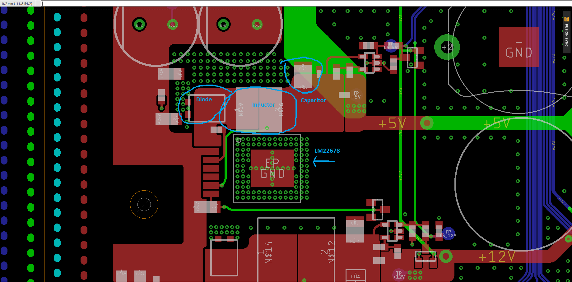
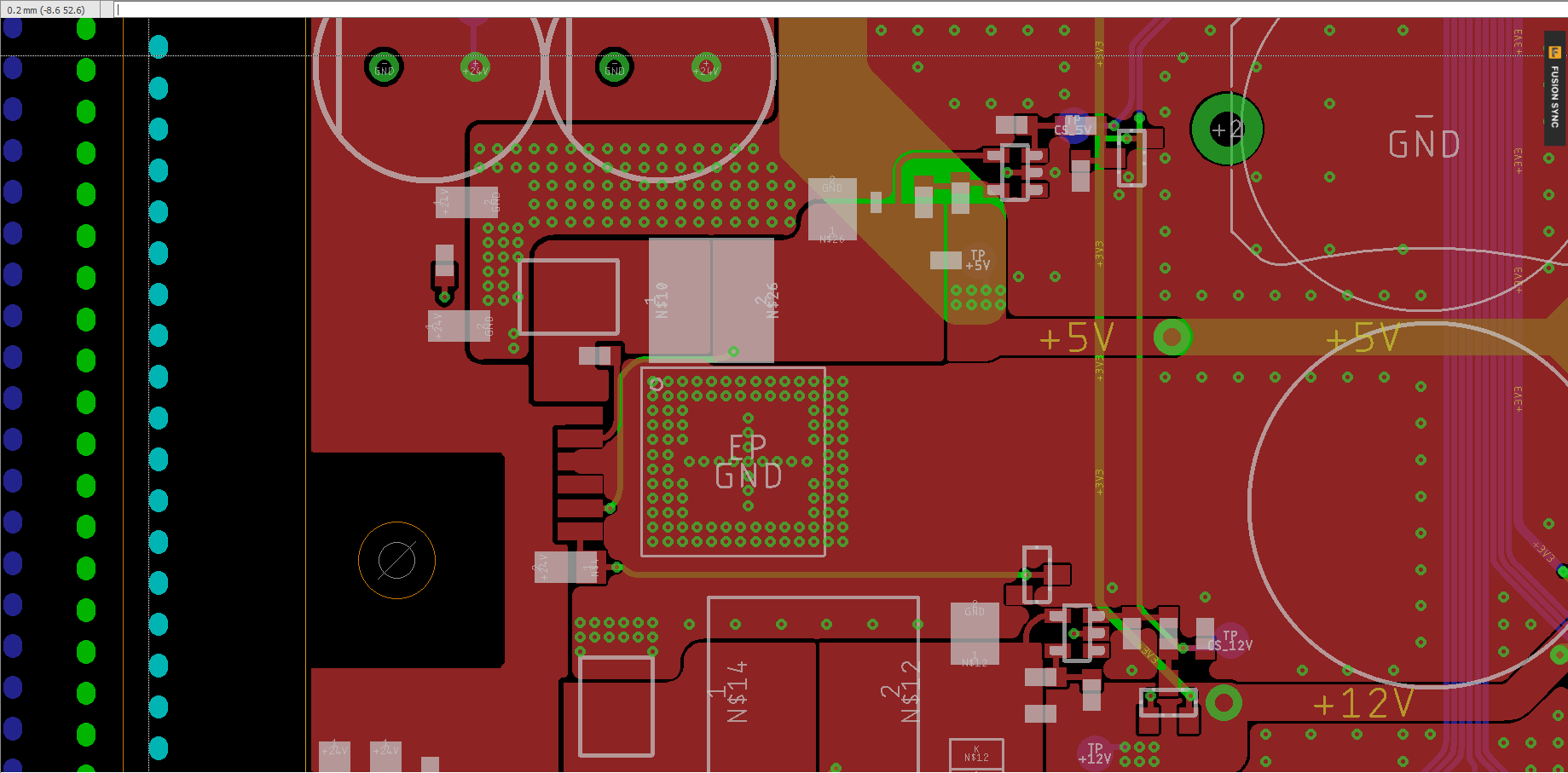
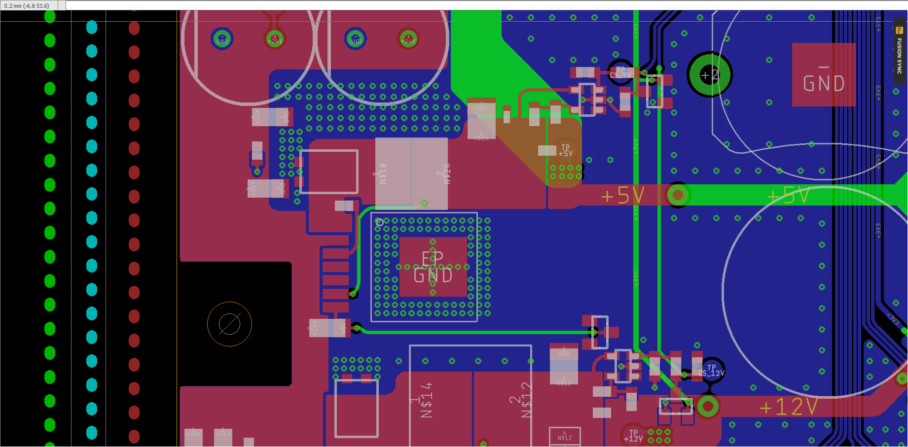
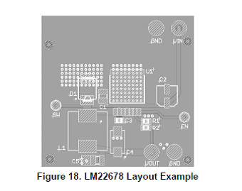
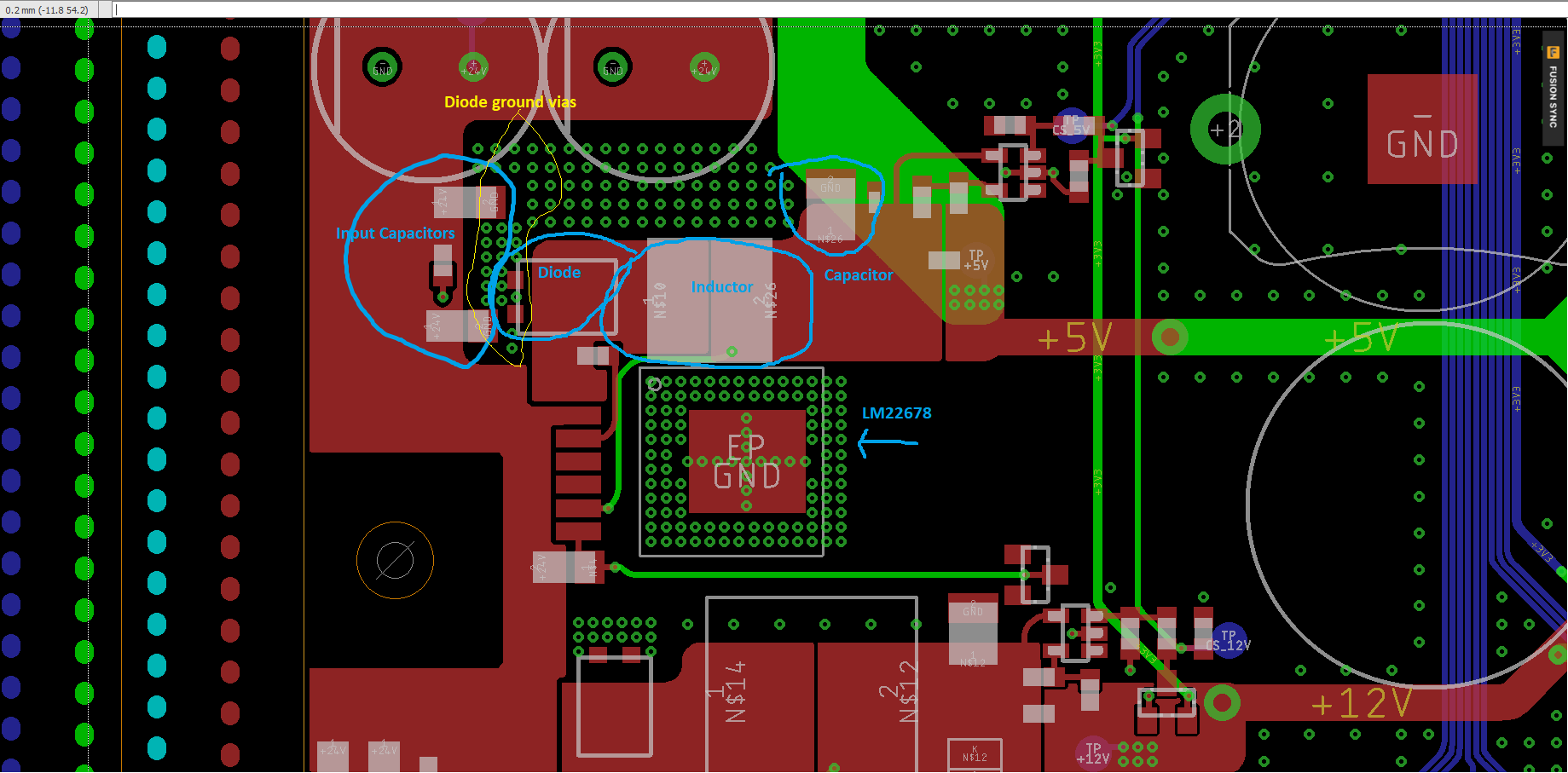
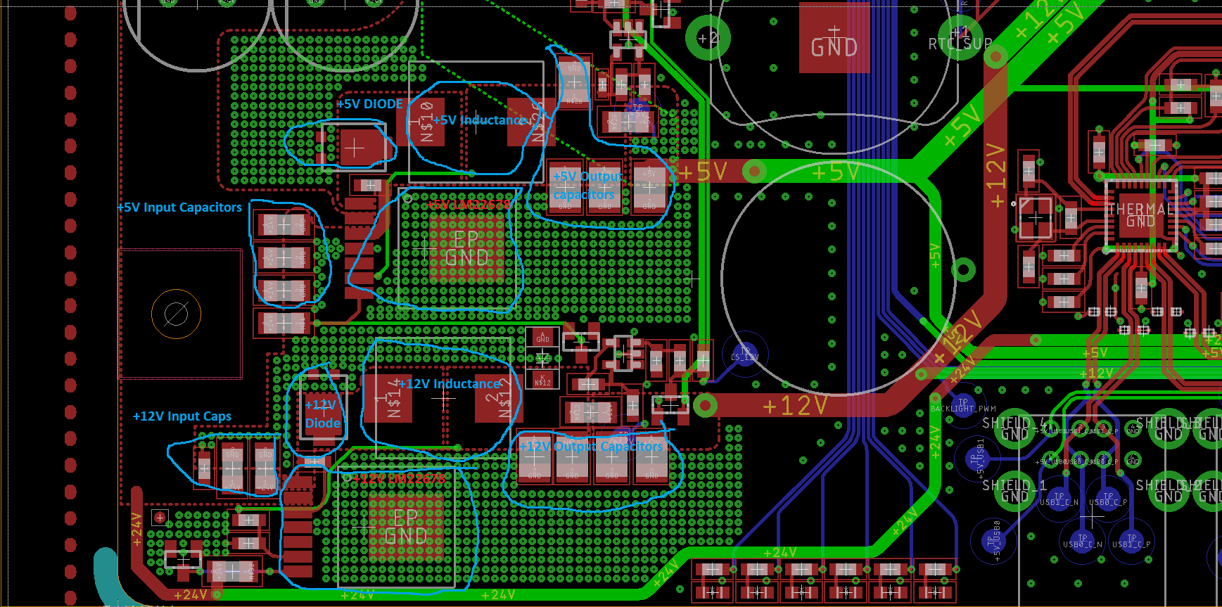
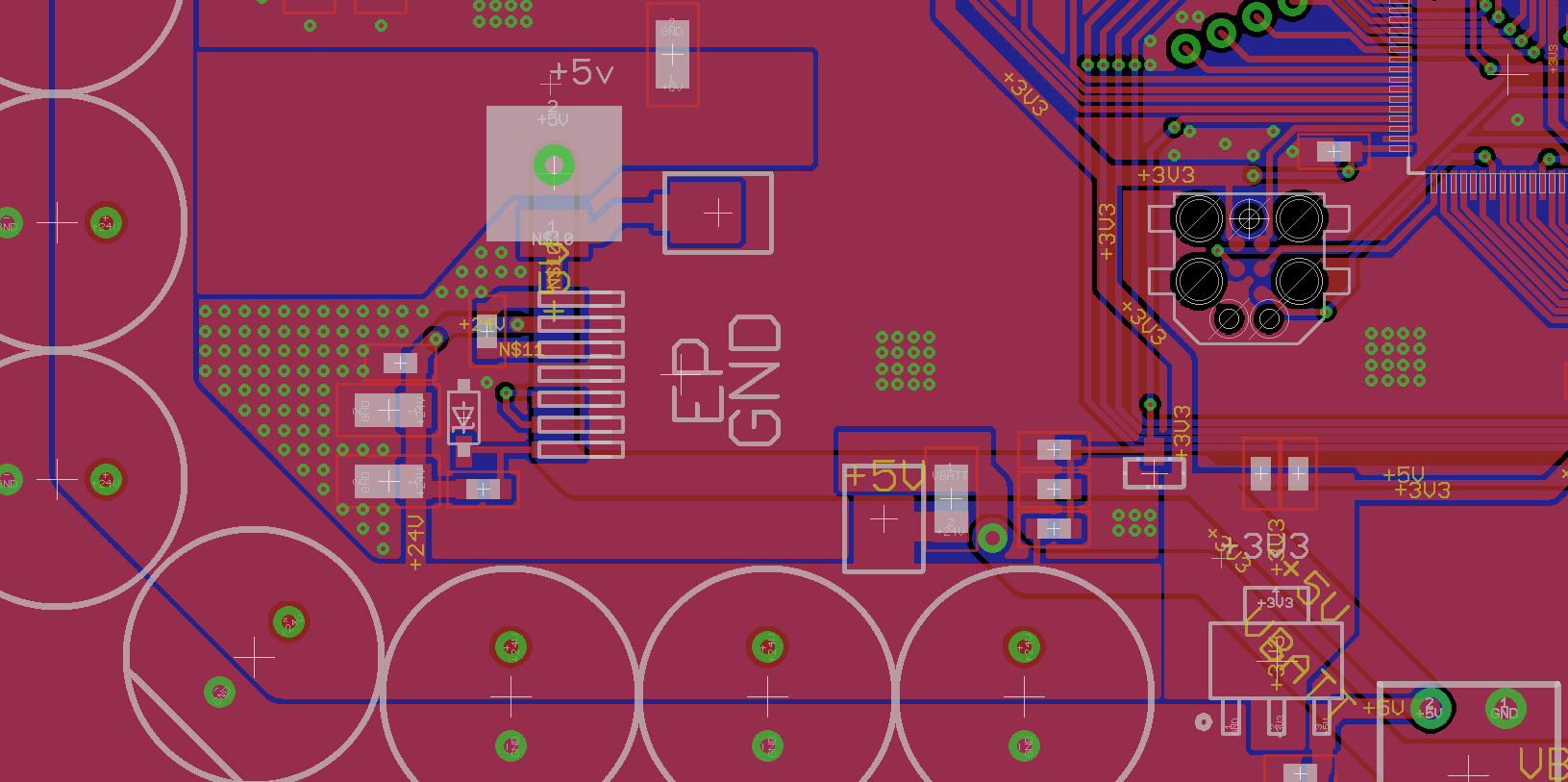
I am developing a board in which I will use 2 LM22678, one to provide +12V, the other one for +5V. You can find the schemes below, generated with Webench and implemented with Eagle CAD.


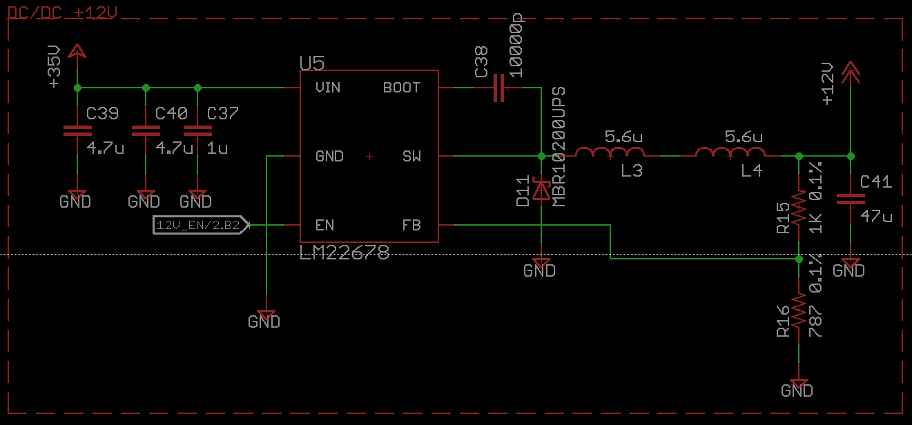
  • The input of the circuit is a 24VAC rectified and filtered through 8 x 680uF Electrolytic Capacitors, obtaining +35V. For the +5V DCDC, when the 35VDC switches off, there is a 10V battery pack (NI-MH) used to provide a soft-shutdown.
  • The diode in both the DCDC is a MBR10200UPS-TP.
  • The inductance is: ASPI-0630LR-5R6M-T15. In the 12V DCDC there is a series of 2 of these.
  • Except for the filter, the other capacitors are ceramics.
  • The enable input of the 5V DCDC is fixed high with a resistor and Zener diode. The 12V can be switched off by a microcontroller.


The layout of the DCDC that generates the +5V is attached below. The load of the 5V is a Display (0.8A), a Raspberry PI3 (0.7A) and an LDO (0.3A) that supplies a microcontroller (overall 1.8A).


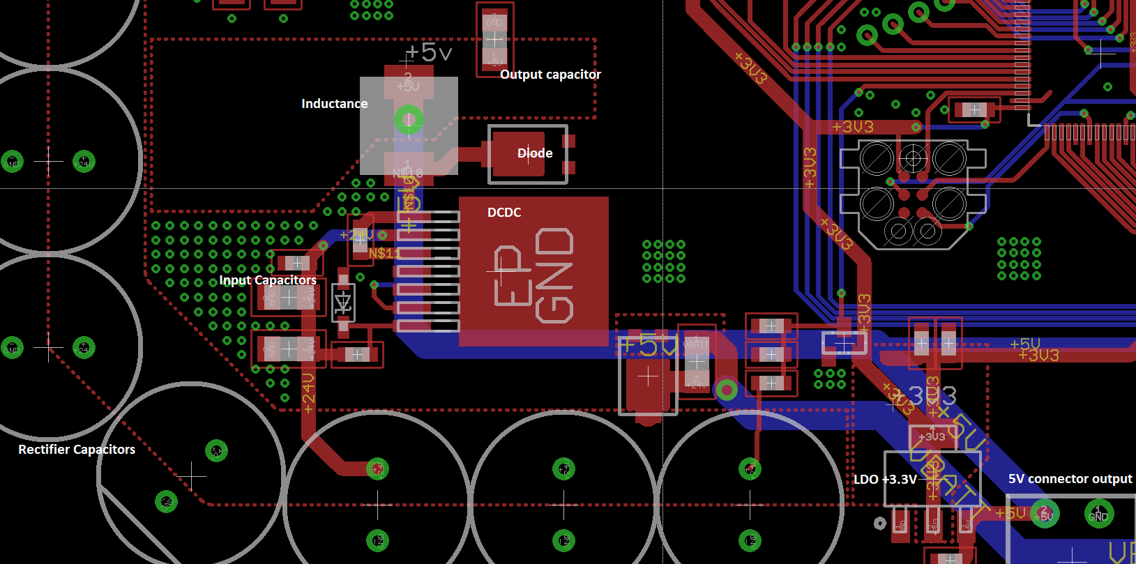
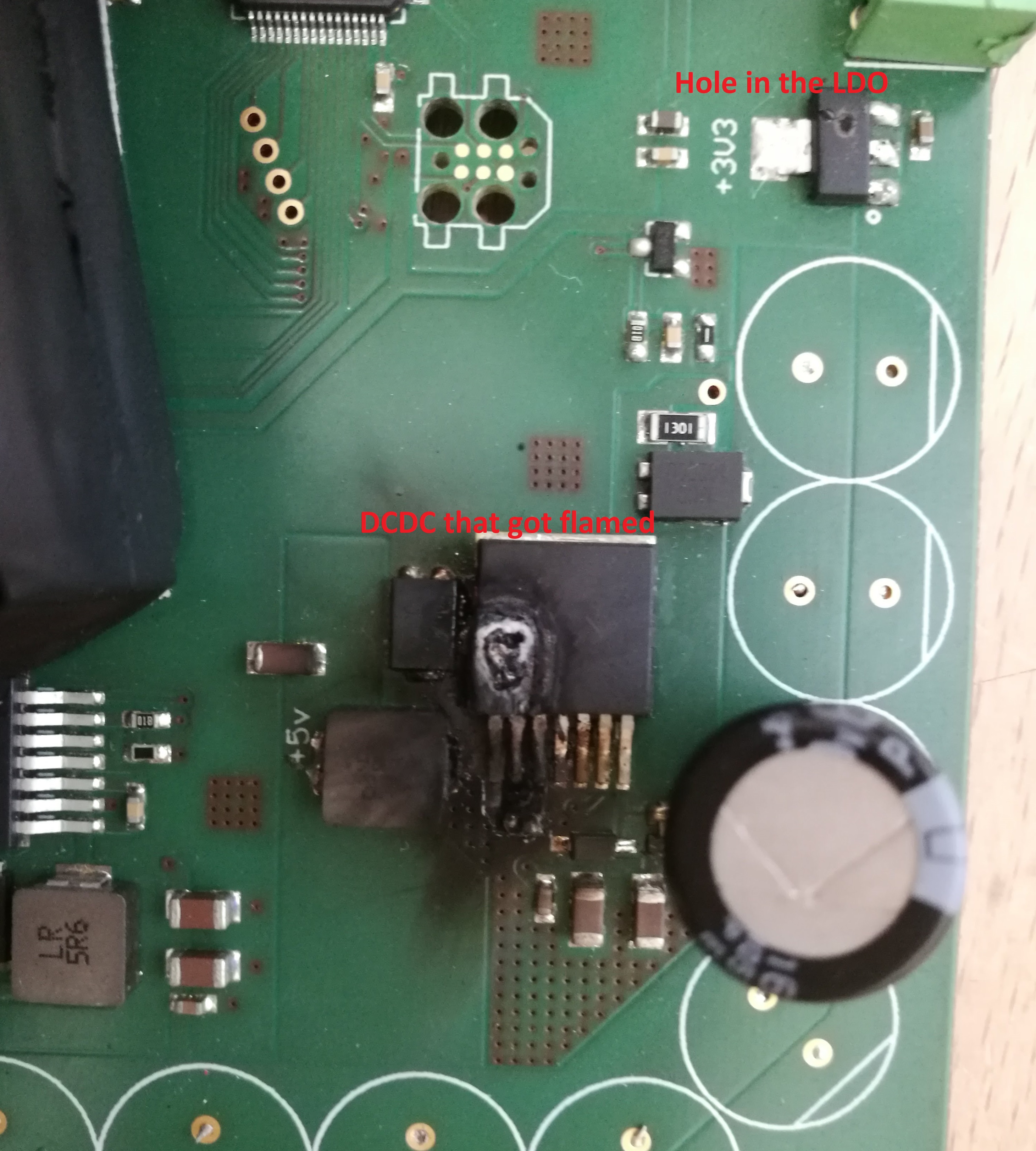
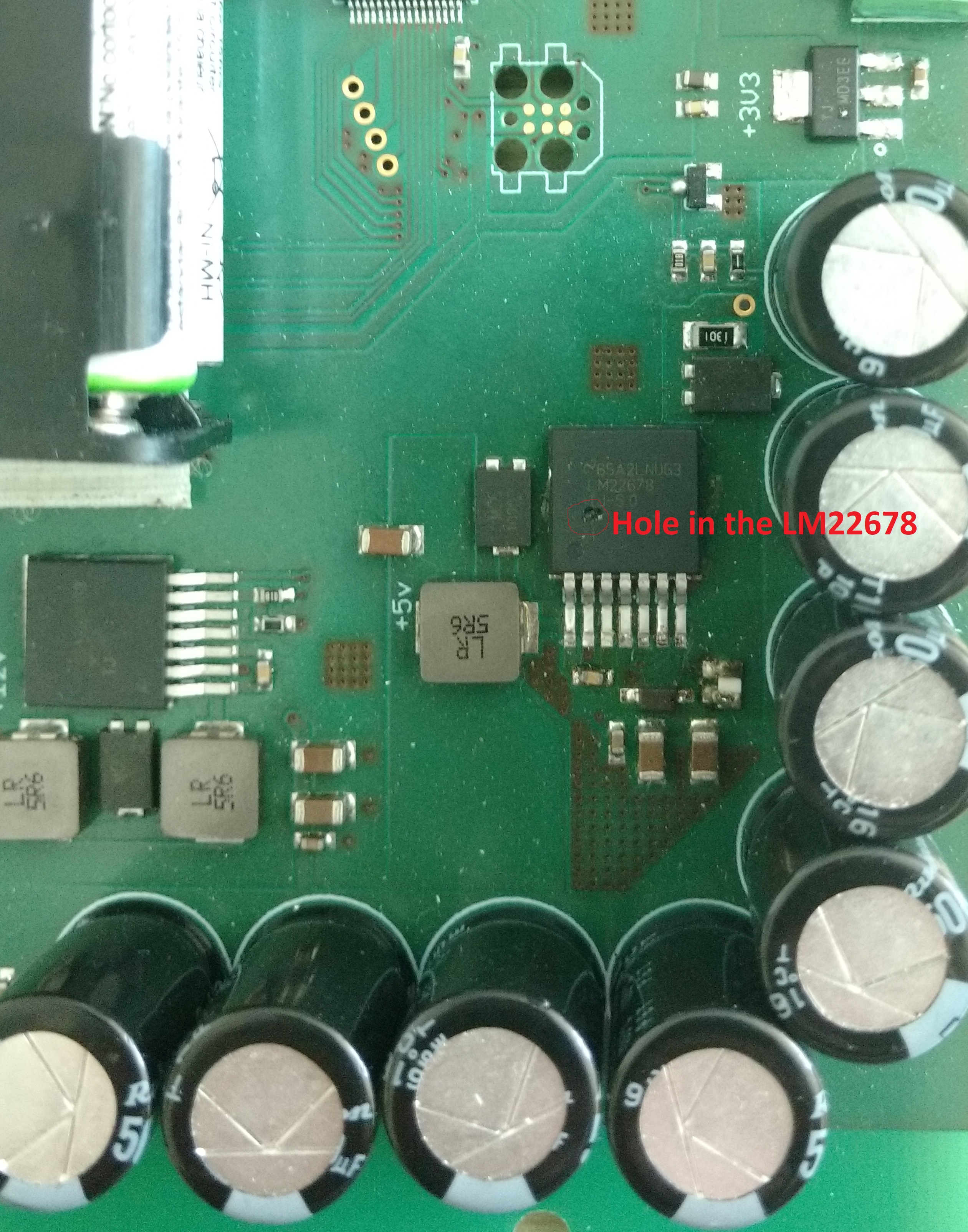
We have 7 prototypes that are in use since May 2017. The DCDC of the 12V never had failures, it works fine. The DCDC that generates the +5V, sometimes, sporadically, has failures. When it fails, also the LDO (TLV1117LV33DCYR) and the microcontroller fails.

The first hypothesis was that the problem was thermal, the DCDC in a box could reach 100°C (212°F). Stressing it, connecting a higher load (1.8A-2.0A, so overall 2.8-3A) to the display supply connector, the temperature grows to 130°C (266°F), and the DCDC goes in protection because of overtemperature. But seems not having any failures. I tried so to disconnect and reconnect this load to the board; the result was that the LM22678 got inflamed (usually, when there is the failure, the board just switches off, but I have never seen fire). So now my hypothesis is that changing the load can creates the failures. I think also the display can be considered a not constant load, and causing, after some time, the failure. The “high load” was connected and disconnected other times before the crash, so it does not happen immediately.

Do you have any idea of which can be the real cause of the failure? Do you have some tests to suggest?
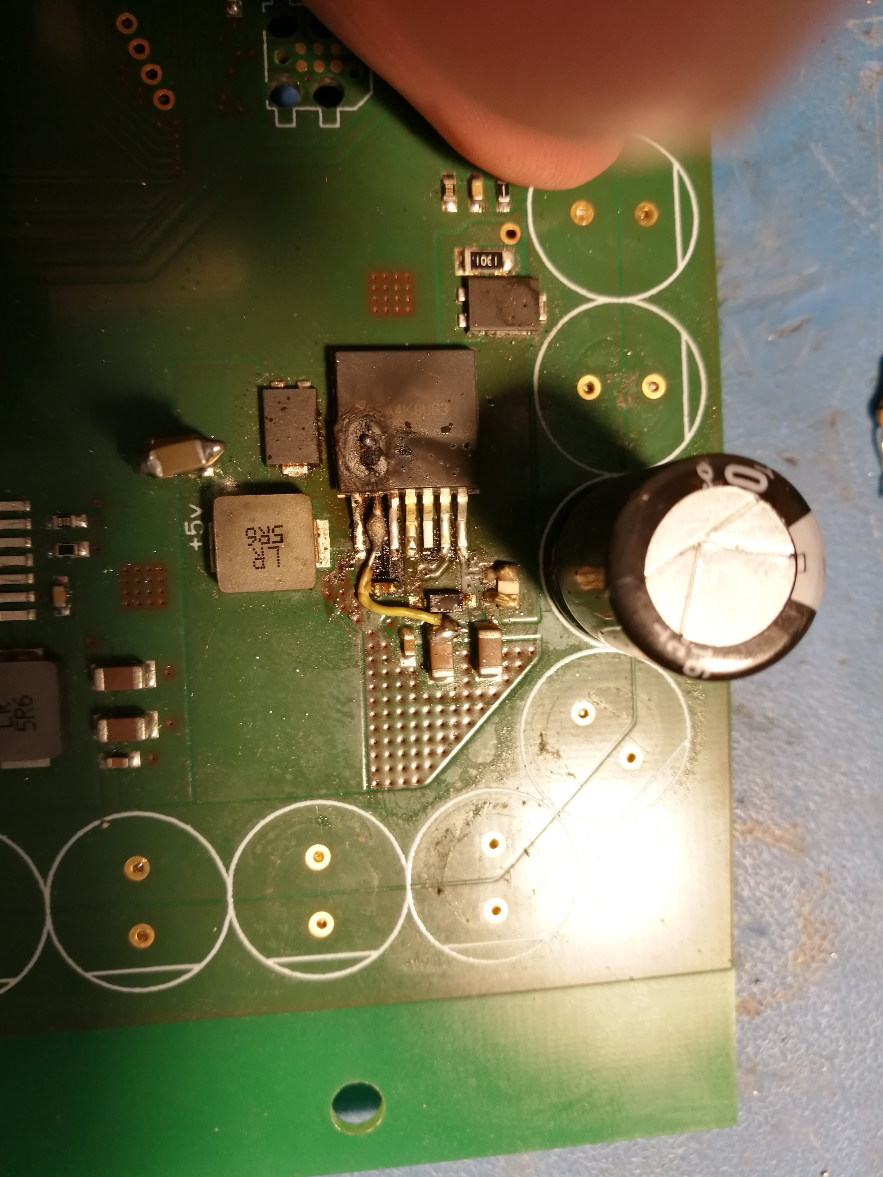
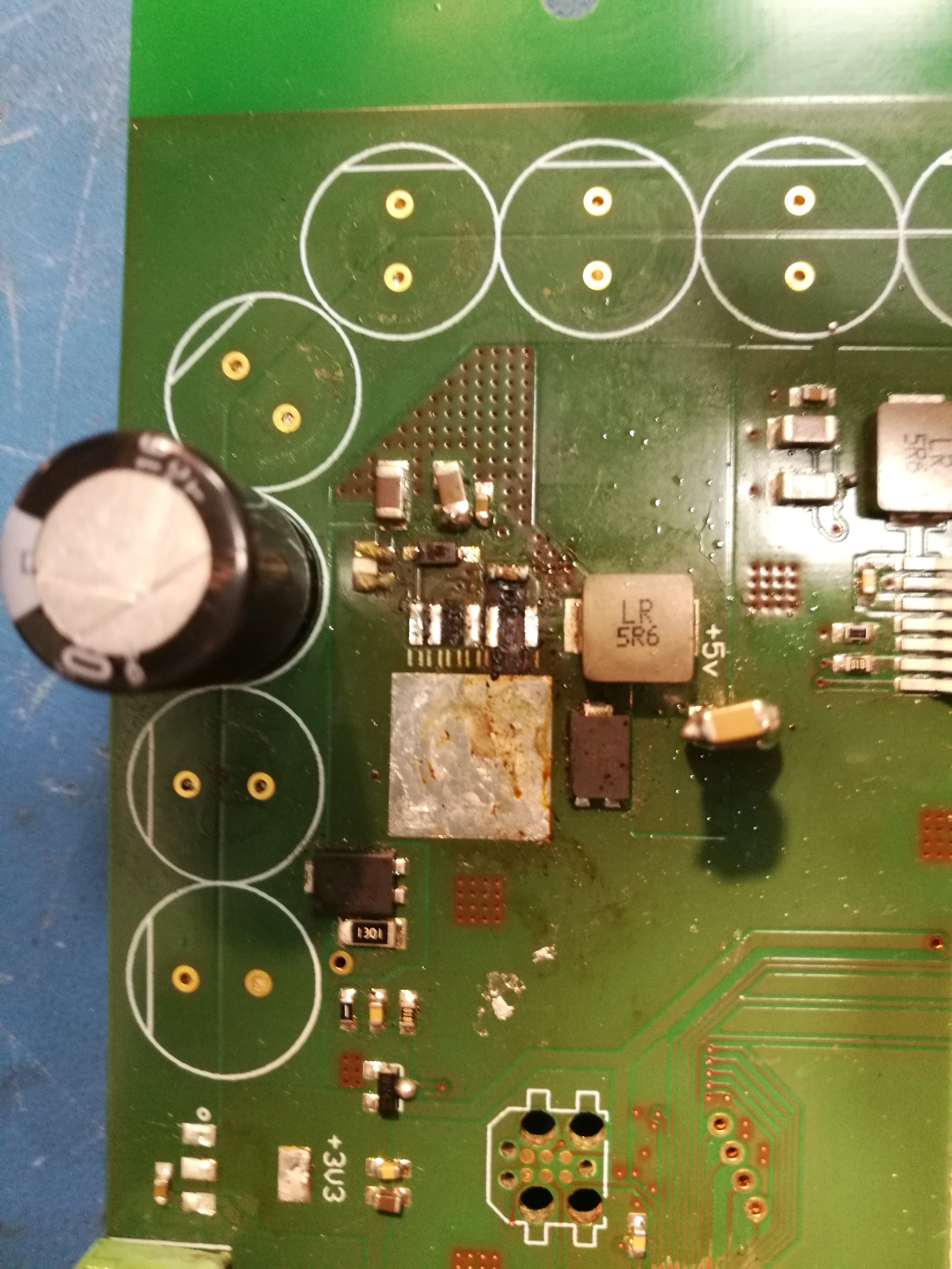
Below there are photos of 3 failured board.


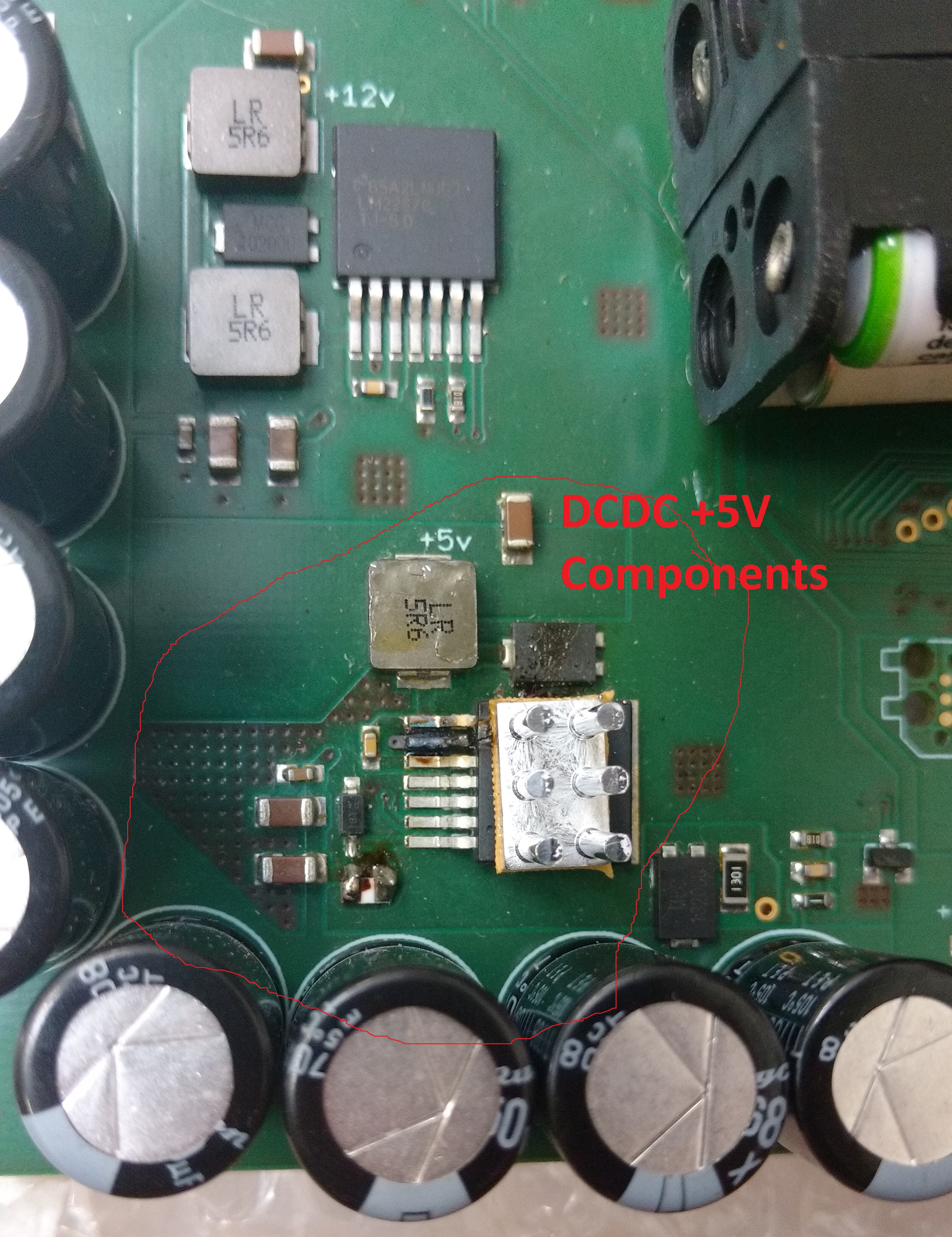
I can send you the components, 3xLM22678 and 2xTLV1117LV33DCYR in order to do a failure analysis. Is it possible?

Kind Regards

  • Hello,
    The type of failure described and shown on pictures attached is typical for over stress conditions.
    In all cases shown it appears that VIN pin on the device is damaged.
    This is only possible if there is significant input voltage overshoot present on VIn pin.
    For this reason it would be helpful to get screenshot of VIN, VOUT and SW node on 5V board.

    The other point in your description that failures happen when load is connected /disconnected is also significant.
    You mentioned what type of load is powered by the device, however distance of load and the way it is connected may also play some role.
    If load is located far away from DCDC power supply, having long line/cable may cause significant overshoot when load is removed and than reconnected.
    Have you tried adding some additional output capacitance and ferrite bead on 5V output?

    In addition i suggest increasing R13 to 470kOhm.

    Hope this helps.
    Best ergards
    Brani
  • Hello,
    I made some other tests. I disconnected all the loads and connected a 25W trimmer resistor to supply 2.6-2.8A. I connected it with long cables. I measured Vin (+35V) and Vout(+5V) both with all the electrolytic input capacitor (5440uF overall) and with only one electrolytic input capacitor (680uF overall). Usually it broke when the capacitors are all connected, but I tryed to removed them, just for the test.

    The preceding plots regard the test with all the capacitor (5.44mF overall). The voltages are the +35V and +5V supplies. You can see the ripple to increment when the load is connected and decrement when disconnected.


    The preceding plots regard the test with only 680uF capacitor for +35V and +5V. You can see that the ripple is much bigger on +35V. On the +5V there is some random noise. I tryed to switch on and off the load some times, and leave it on for some other time. After some seconds (30-50) it was on fire again.

    After that I noticed that the 100u output ceramic capacitor on the +5V line was much lower in capacitance (because it is X7R). So i added a lot of output ceramic capacitors (130uF effective overall) and made again the test with 680uF input capacitance. But it burned again. Before of that it restarted some times because of the overtemperature. You can see the plots below.

    In this case the plot start with the load connected, then the load was disconnected, after reconnected and then removed the supply. It is the +35V supply.


    This is a zoom on the 5V with load on. I think that noise is caused by the internal mosfet switching. I placed the oscilloscope's probe as close as possible to the dcdc.


    The input voltage seems good, not having overshoot. It should be strange that the problem is in the input voltage, because the other LM22678 that generates the +12V supply never broke.
    Can the problem be caused by the other components? The part number of the diode is MBR10200, the inductor is ASPI-0630LR-5R6M-T15. 
    Do you have any other ideas or test to suggest?

    The following photos are the taken after the second broke, the one with larger output capacitors.


    Thank you for the support.

    Lorenzo


  • Hi Lorenzo,
    Thank you for additional data/screenshots.

    It looks like your supply is fairly stable and I don't see any significant "swings' that could cause behavior you are reporting.

    As far as other components are concerned I think the focus should be on following:
    1. I would suggest increasing inductor value to 10uH. You may even use inductor from the same series as currently used, only with slightly higher inductance., for example ASPI-0630LR-100.
    2. Since you see failure on the device that is converting 35V --> 5V, (~14% duty cycle), low side diode will be on most of the time. That puts an additional stress on the diode used, so i would suggest trying diode that can handle slightly higher current. Here it should be noted that on board pictures you provided i don't see any ground vias placed directly underneath IC and on the ground side of the freewheeling diode. This greatly reduces potential for heat dissipation in your design. Please check device datasheet, section 10.1, for suggested layout.
    3. What is the total estimated output capacitance in your design? Excessive amount of output capacitance can have negative effect on device performance. According to my calculations effective 100-120uF of output capacitance should be sufficient for your load conditions.

    I hope this helps
    Best ergards
    Brani
  • Hi Brani,
    Thank you for the support.

    1) I tryed to increase the inductor value, with this one: ASPI-1040HI-100M-T05. It is bigger but the PCB is big enough to place it. At the beginning I tried to cool down the DCDC with a big Fan 300mm diameter, and in this way the dcdc's temperature was 70-85°C (158-186°F). It worked for some hour without any problem. So i decided to stop the fan. The temperature increased and the DCDC began to restart for overtemperature. I switched it off because I was sure that if i leaved it switched on, it would fail again. 
    2) I have bought some 15A and 20A schottky diodes (DST2050S, DST1545S) to test the DCDC with them. I will test them as soon as possible. Why do you think the diode can be the problem? Of course the diode will be on for most of time, but can this be a problem for the DCDC? Your suggestion was about a possible life reduction of the diode?
    3) In the last tests there was 6x100uF 1206 ceramic capacitors. According to the datasheets, at 5V the effective capacitances were for 1 33uF, for the other 4 22uF (there are 2 different part number). So the total amount of capacitance is (22*4 + 33)uF = 121uF. In future i think that I will use an electrolityc capacitor.

    In the second prototype i made a different routing for the DCDC. It is shown in the photos below. The PCB will be 4 layer. In the bottom layer and the second layer the ground planes are extended everywhere. In the third layer and in the top one they are big too. I left a rectangle out of the stop mask in the bottom of the circuit under the 2 DCDC, so it is possible to install an heatsink in the bottom.


    Do you think this will be a good way to have a good heat dissipation? Do you have any other suggestion for the layout?

    Do you have any other tests to suggest?

    Thank you very much
    Best Regards
    Lorenzo

  • Hello Lorenzo,

    The ideas proposed above were targeting most of the external components used in your design,so that the root cause could be identified.

    From your description it sounds like the issue could be related to thermal performance for 35 to 5V conversion circuit. Please see screenshot from device EVM regarding layout for optimal thermal performance. It is strongly recommended adding multiple thermal vias in the area of exposed pad on the IC as well as under re-circulation diode.

    Layout you are showing in the post above looks better that the initial PCB layout. However i think it would be beneficial to have more vias in the exposed pad of the IC and also on the diode. As much as i can see there are no thermal vias underneath diode. We are also recommending to select diode with exposed pad for improved thermal performance. Having solid copper pour on top and bottom layer will help with heat dissipation.

    In the layout are providing i don't see any input capacitor near the IC. It is extremely important that at least small bypass capacitor (100 nF or similar) is placed close to the pins on the IC that should be decoupled (in this case between pins 2 & 4). Large pulsing current is going through Vin/GDN pins and proper decoupling is very important for proper functionality.

    Have you manufactured new board or there is till a chance to make some layout changes? if you can make changes please provide layout file for review and comments.At this point i feel like we need to verify device performance with improved layout in order to make any conclusion as root cause is concerned,

    Best regards

    Brani

  • Hello Brani,

    I repost the previous photo adding some details. I highlighted:
    - The input capacitors, do you think that in that position they are too far from the DCDC? They are 10uF overall.
    - The ground vias of the diode. The ground pins are the 2 highlighted near the via. Do you think there are not enought via?

    The first 3 board are manufactured. Tomorrow I will add all the components and start some tests. The board can of course be modified before be produced in big quantities. I think i could move right the diode and the inductor for have more ground plane near the diode and move down the input capacitors. I can send you some photos when I will finish the last version.

    About the vias under the LM22678 thermal pad: if the are a lot of via under it, can the stagnum pour into them, creating some soldering problem to the component? If you think that this cannot create problems, I of course can add vias on all the thermal pad area.


    Thank you for the support!

    Lorenzo

  • Hi Lorenzo,

    Thank you for this layout screenshot.

    It certainly looks better, however i have some recommendations:

    1. Input capacitor is too far away form the IC pins. If possible place small bypass capacitor (47 or 100nF) very close to the pins that it suppose to decouple (2 & 4).
    2. For best results i strongly suggest to try to replicate layout on the device EVM. This is proven and tested layout which should allow you to move faster with your design solution with minimum number of corrections needed.
    3. Regarding thermal vias in ground pad: Feel free to add some more vias in the exposed pad. You are currently showing sibgle horizontal and vertical row of vias. I would suggest to minimum double or triple number of vias in x/y direction.

    Looking forward to your update with new board.

    Best regards

    Brani

  • Hi Brani,
    I tryed to replicate as similar al possible the scheme, but the input and output direction added difficulty. These are the photos:


    Without planes, all layers


    Top with plane


    Top and bottom with all planes except ground plane.

    The ground planes are in all the 4 layers, the input capacitance are nearer to the input pins, the 5V inductance is bigger (10uH), and I added some output capacitors 1210 (130uF for 5V, 47uF for 12V). I added a lot of vias.

    What do ou think about it?

    Kind regards

    Lorenzo

  • Hi Lorenzo,
    I think this layout looks much better.

    However i have couple of suggestion:
    1. Swap position of 5V inductor and circulation diode. this will allow for much tighter ground loop between input and output
    2. make sure your input power supply is not hitting current limit. The reason for this is that you see big ripple on input when load is applied . This indicate that your input power supply might be hitting current limit.

    Other than this layout looks much better.
    Bets regards
    Brani