This thread has been locked.

If you have a related question, please click the "Ask a related question" button in the top right corner. The newly created question will be automatically linked to this question.

TPS25927: Not able to drive EN/UVLO pin high

Part Number: TPS25927

I have implemented the TPS259271 in a new design, and I am in the process of bringing up the newly built boards.

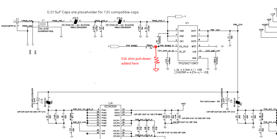
I have another device driving the EN/UVLO pin with an open collector driver and a 100k pull-up to 12V at the TPS259271.  EN/UVLO is held low until a user button is pressed.

The TPS259271 appeared to be functioning normally, but after repeated power cycles where the power is being enabled only for less than a second, the device stopped responding to the enable signal.

The resistance measured to ground at the EN/UVLO pin was less than 20 ohms, and the pull-up was no longer able to pull the signal above the 1.4V threshold.

This was observed on two units, and a careful review of the datasheet revealed that the maximum voltage on this pin should be <6V.  This was my mistake.

So I modified a third unit to implement a voltage divider at the EN/UVLO pin using a 51k ohm pull-down and 100k ohm pull-up to 12V.  I verified the resistances after the rework in the powered off state.

On the very first power-on, the TPS259271 failed to pass power through the e-Fuse, and the node now measures <10 ohms to ground in the powered off state.

Can you provide any additional guidance on how to get this circuit to work?  Once this input stops functioning, I assume that some irreversible damage has occurred.  Can you confirm?

Thank you,

Todd

  • Hi Todd,

    What is the load (capacitive ?) during power cycling at the input?
    Have you seen failure only at EN/UVLO pin for the first two cases? Is the MOSFET fine?
    I will check with the design team. In the meanwhile, can you repeat third test (using voltage divider at the EN/UVLO pin) on another TPS259271 device.

    Best Regards,
    Rakesh
  • I have a 2.2mF and 10uF capacitor on the output before it goes to two 6V regulators that have 66uF at their inputs, for a total of 2.342mF.

    The DV_DT pin has a 0.0022uF capacitor to ground, and the ILIM pin has a 121k ohm resistor to ground.

    I am reluctant to try the experiment until I have exhausted my other options for investigating this circuit, since I only have 5 prototypes, and I have already used 3 at this point.  :P

    I am currently providing power to the power connector from a benchtop power supply with the current limit set to 0.50 amps, and when I was able to turn on the power successfully with the previous two boards, the current consumption in the ON state was less than 200 mA.

    Circuit diagram added below.

    Thanks for your support,

    Todd

  • Hi Todd,

    Few comments on the schematic.
    121k ohm RILIM resistor sets current limit to 4.33A not to 2.54A mentioned in the schematic.
    As you are driving 2.342mF load capacitance, you need to use higher than 0.0022uF at DV_DT pin. A minimum of 33nF is required as per design calculator. Please use design calculator available at www.ti.com/.../toolssoftware
    what is the intention of doing power cycling? Does the design need to qualify for "power fail test"? If you intent to do power cycling with large 2.342mF load capacitance, the body diode of the device will be stressed during the load capacitance discharge. I recommend to use external blocking FET at BFET pin.
    In your schematic, the filter components can add substantial inductance at the input of TPS259271 device. Recommend to add TVS at the input to avoid violating abs max voltage rating during any transient events. Please refer Section 10 in the datasheet.

    On the third board, you mentioned "the TPS259271 failed to pass power through the e-Fuse". What is the test condition? Have you verified whether the device is turning OFF due to fast-trip?

    Best Regards,
    Rakesh
  • Thanks, Rakesh.

    The power cycling was being performed because a downstream circuit was not functioning properly and shutting down power by deasserting the enable pin.  I was repeating the cycle as I investigated the downstream event.  

    I will update the board and schematic to use a 69.8k ohm resistor which should change the limit to 2.794A.

    I will also update the board and schematic to use a 47nF cap to limit the inrush current, and I will consider adding the TVS diodes in a future revision of the board.

    We had hoped to avoid the need for an external blocking FET.  Is there a recommended time between power cycles that we should try meet if I make these changes?

    I have an LED directly tied to the 12V that is enabled through this e-fuse, and the LED did not light up when I pushed the power button.  When I measured the resistance at the EN_UVLO pin, the value was less than 10 ohms where it had been ~50k ohms before the button was pressed.

    If I make the changes to the ILIM and the DV_DT components, and add the voltage divider to the EN_UVLO input, do you believe that we are ready to try powering the circuit again?  Do you think there are any other measurements or things to check before we risk powering on another board?  I would hate to damage another of these parts.  Do you think it is more likely that the lack of the TVS diodes or the fast DV/DT setting caused the failures?  If it more likely the inductive transients, then I will need to make sure that I add the TVS diodes before trying this again.

    Thanks,

    Todd

  • Hi Todd,

    Thanks for the details.
    I suggest configuring ILIM, DV_DT values, resistor divider at EN_UVLO input, place TVS diode before any further testing. Make sure that you are clear on the issue with the down stream circuit. For the first time power up, if possible disable the down stream circuit and see whether 12V is coming or not. Capture Vin, Iin, EN, Vout during power-up.
    If power cycling is must in your application, I recommend to use TPS25940A in your future revision of the board.

    Best Regards,
    Rakesh
  • Hi Rakesh,

    The TVS diode is on its way so, hopefully, I can test again next week.

    Power cycling should be a rare event with this device, but if I need to give technicians guidance on using the device, is there a recommended period between power cycles that I should be aware of when using the TPS259271?

    Thanks,

    Todd

  • Hi Todd,

    During power cycling, current can flow from the output to the input through the internal body diode. The body diode of internal MOSFET is not expected to support high current for long duration. It should be able to handle <5A for short duration (<10 us) and small current (< 100mA) for long duration.
    Because of load capacitance if you expect higher body diode current for long intervals, consider placing series diode to block reverse current while testing.

    Best Regards,
    Rakesh
  • Thanks, Rakesh.

    The power cycling I was describing was not removing the input power.  It was only enabling or disabling the internal MOSFET.  The input voltage source was maintained through the power on-power off cycle, so I believe the current flow from the output to the input would have minimal if any.  We still had the problem with the inrush current, that we will address with the dv/dt setting.

    By my calculations, in circumstances where the power from the AC/DC converter that sources the power is removed, the resulting reverse current through the body diode will be in the <100mA range (12v / 150k -> 80mA).  We will do some measurements in the lab to verify this, but with this in mind, my conclusion is that the series diode to block reverse current should be unnecessary.  Do you agree?

    Thank you for your support,

    Todd

  • Hi Todd,

    Understood. If device enable/disable is through EN pin, there will not be much reverse current. So, series diode is not needed to be in place for testing your prototype board.

    Best Regards,
    Rakesh