This thread has been locked.

If you have a related question, please click the "Ask a related question" button in the top right corner. The newly created question will be automatically linked to this question.

UCC27524: INB to OUTB logic wrong

Part Number: UCC27524

Hi,

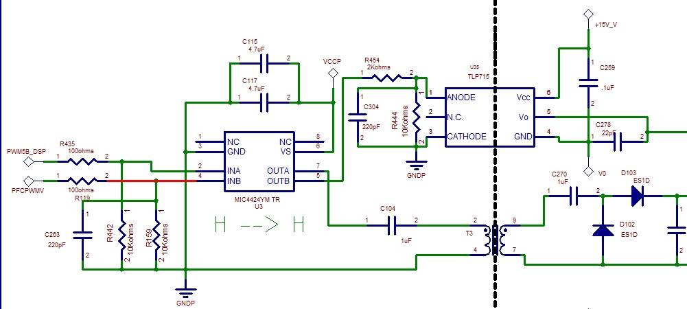
We have designed in UCC27524 in a customer to replace MIC4424. The schematic is as below. UCC27524 is used to do the isolated gate driver along with transformer and optocoupler to drive the MOSFET.

During the aging test, it's observed OUTB remains low no matter INB=0 or 1. INB is from C2000 PWM port. INA and OUTA is always good.The failure analysis done by TI says that it's caused by EOS.

I wonder if you could help review the schematic and tell me if any part is designed improperly, and if any modification is needed to extenuate the problem.

  • Hello Howard,

    Thank you for the interest in the UCC27524. I am an applications engineer in the High Power Driver group at TI and will help to resolve your concerns.

    I would like to get a little more information on the circuit operating conditions to be able to comment and make suggestions.

    Can you provide the voltage level on VCCP, which is VDD of the driver? What is the operating frequency and maximum duty cycle of INB/OUTB? What is the input signal amplitude to the INA and INB inputs? Also can you describe the conditions of the aging test, operating ambient temperature(s), any humidity conditions, does VCCP level change?

    Also you mentioned that there was an FA report from TI, do you have the FA document report number so I can review the report?

    With some information I believe we can determine how to resolve the concern.

    Regards,

    Richard Herring

  • Richard,
    VCCP=12V, VDD is pin6 in the schematic, it's pin to pin with MIC4424, so the schematic is not changed.
    frequency of INB/OUTB is 22k, maximum duty cycle is 90%. INA and INB are 3.3V signal.
    During the aging test, temperature is 40℃, humidity should be the same as outside around 50%. They didn't monitor VCCP during the aging test, they only measure it after the problem was found and it's the same as 12V.
    The FA report number is QEM-CCR-1712-00052, I will also send an Email to you in case you can't find it.

    Howard
  • Hello Howard,

    Thank you for the details on the schematic and operating conditions. With VDD =12V and output B driving the input of the optocoupler with 2 kOhms in series the output B driver current is well below the IC ratings. VDD at 12V is well below the IC ratings. I do not see concerns with your description so far regarding output B conditions. I would like to know what is the load on the output of the gate drive transformer connected to output A; at the D102 and D103 connections.

    I will review the failure report and research the details to get more information on what part of the IC may be damaged. This may take 1 or 2 days to confirm the information in the report.

    Regards,

    Richard Herring

  • Thank you. Waiting for your idea.
    at the D102 and D103 connections it's G and S of MOSFET.
  • Hi Howard,

    I am closing this thread since we are working the issue via email.

    For others searching this thread, my assumption is the issue is due to either false triggering of the chip, or dv/dt issues damaging the chip.