This thread has been locked.

If you have a related question, please click the "Ask a related question" button in the top right corner. The newly created question will be automatically linked to this question.

WEBENCH® Tools/LM76002: Output power ripple issue when input is at 5.6V

Part Number: LM76002

Tool/software: WEBENCH® Design Tools

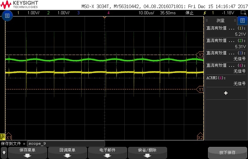
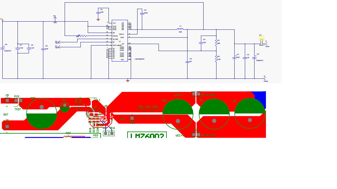
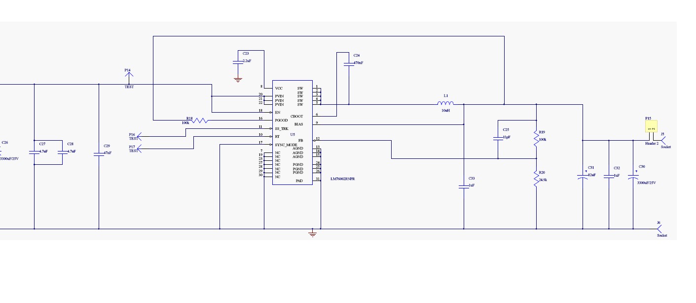
we are evaluating LM76002  for our smart power grid project , but we found output power ripple issue when input power source is at 5.6V(our output is 5 V). Is it a known issue? or is there any suggestion to fix it?

thanks a lot. 

  • Can you specify the details of the issue? Picture would be helpful. Thanks.

    -Yang
  • please refer to schematic and layout we are using, L1 6.8uH, C31 100uF, C30 no mounted.

    channel 2 is the input , channel 1 is the output.

  • Hello,
    Your schematic/ layout picture is really hard to read.
    Here are initial observations:
    1. it appears that there is no small (47 or 100nF) decoupling capacitor placed close to the IC. It is very important to place this capacitor between VIN & PGND pins to reduce amount of high frequency noise. Please place this capacitor as close as you can to the IC and check output signal.
    2. Ground return is very long. For optimal performance input and output capacitors should be connected to create very tight loop. This helps with minimizing loop inductance and improving overall performance (especially for EMI).
    3. ground side of input and output capacitors should be connected with multiple vias to solid ground plane. Form provided layout it is not clear if this is done or not.
    4. feedback signal routing is very critical. This signal should be routed as far away as possible form noisy nodes (for example switch node)
    5. Measurement technique can greatly affect measured waveform. Make sure that you use oscilloscope probe with very short ground loop (preferably differential probe) and measure directly across output capacitor.

    Hope this helps.
    regards
    Brani
  •  Hi, Brani

         Thanks a lot for your feedbacks,  Here I attached our schematic again, hope it helps you understands our design,  we exported Layout from WEBENCH.

    we do have on decoupiing capacitor C29   between VIN & PGND.  I will move C29  more close to LM76002, then test again.

    one more comment for our design , VIN is not a stable source , it will change from 5.5V to 48V, output is 5V, but system load is almost under 500mA.  in some case , system load may up to 1.5A or 2A.

    we planned to evaluate LM76002 EVM board  since we ordered one LM76002 EVM , we havn't got it after one month waiting yet.  

  • we rested after we move  C29 more close to LM76002, the Ripple  on SW is reduced to about 300mV VPP,  we will keep optimizing it.  We will test it  on LM76002 EVM  also after we get the board.