I am debugging a set of LM25085 based buck power supplies. They are both doing the same thing, but let's start with the +5V version.
Here is the schematic:

This had originally been generated in WEBENCH, but I've made a few changes on the board to improve possible issues that there may be in the layout, design, etc.
Following a few posts I've read, I increased the input capacitance to around 50uF. C8 is also DNP. In an attempt to rule out a bad kelvin connection in the layout, I increased R12 to 3.32k (imagine that).
This power supply works very well without load. It regulates slightly above +5V with little to no spikes (with a +15.5V input). My issue is that any kind of load or increase in Vin will crash the supply down to an improper voltage and nothing will fix the output until the load has been removed and the power supply has been power cycled.
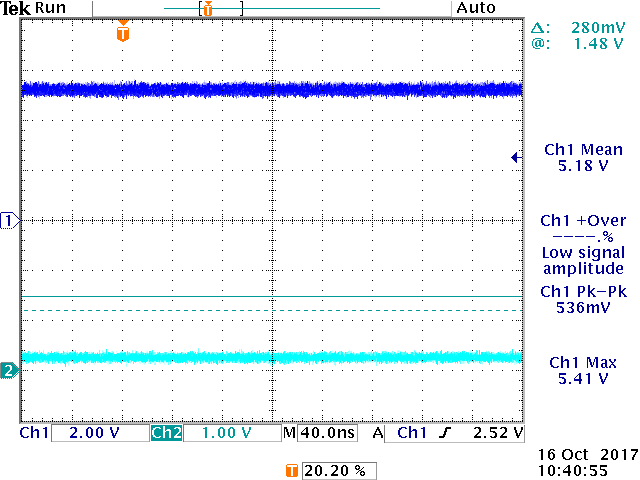
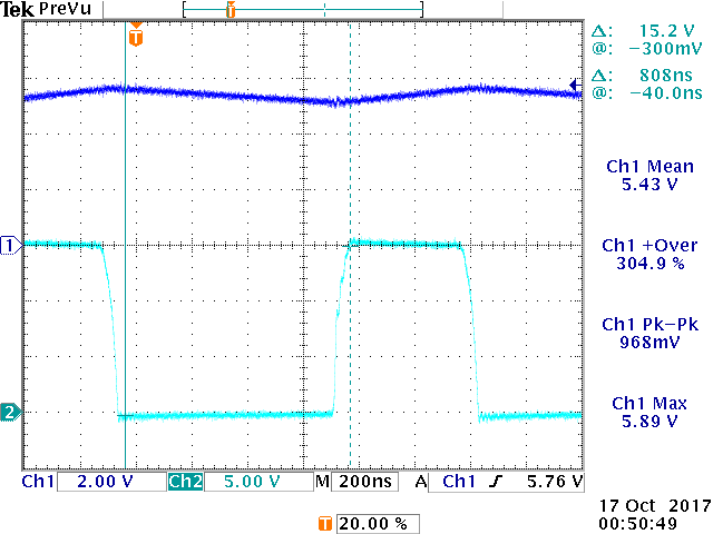
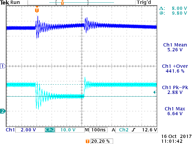
That is pre-load (CH1). The next image is what happens when the load is introduced (CH1 output, CH2 gate):
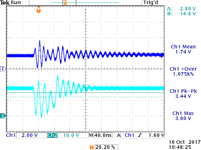
This is a zoom in of the ring I have been observing when the chip enters this state. I assume this is a parasitic issue, but have tried my best to address what I can. What concerns me is that there is no recovery once the load is removed. My primary concern is that diode D4 could be affecting regulation by resonating with the switch cycle per 8.2.2.9 of the datasheet.
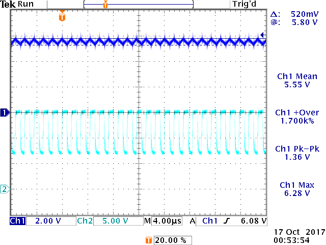
If I decrease the supply VIN to +12V, then I have a fairly ugly output, but the power supply remains in regulation with the load out to 2ish Amps no problem. That particular test seemed to rule out my kelvin connection concerns. The connection is not ideal, but also not too bad.
My leads for measuring are longer than normal for safety reasons, but when I do the measurements right at each node manually, the ring is still there (with slightly lower amplitude).
I am going to run through adding some gate resistors to slow down the P-CH fet and slow down the turn-on time of the FET. Any other advise may help, I imagine a ring of this magnitude will be detrimental to downstream components, even with CMOS.. This power supply is also supposed to run up to 24V, so it will need an update, for sure.
This problem is similar to this post:

I suspect they had similar issues, but did not address the FET turn-on time issue they may have had.
Remember, this problem is directly related to VIN.
Nick