This thread has been locked.

If you have a related question, please click the "Ask a related question" button in the top right corner. The newly created question will be automatically linked to this question.

TPS63061: strange death when applying 12V

Part Number: TPS63061

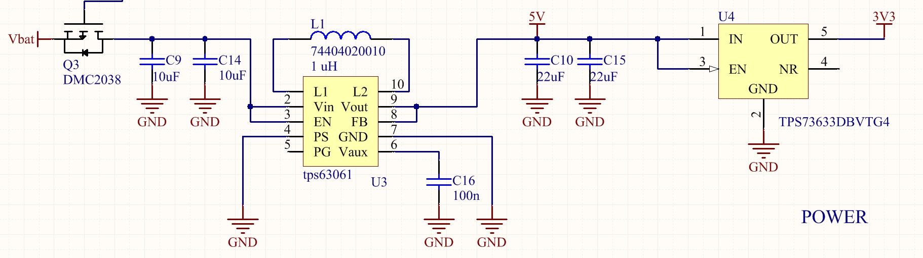
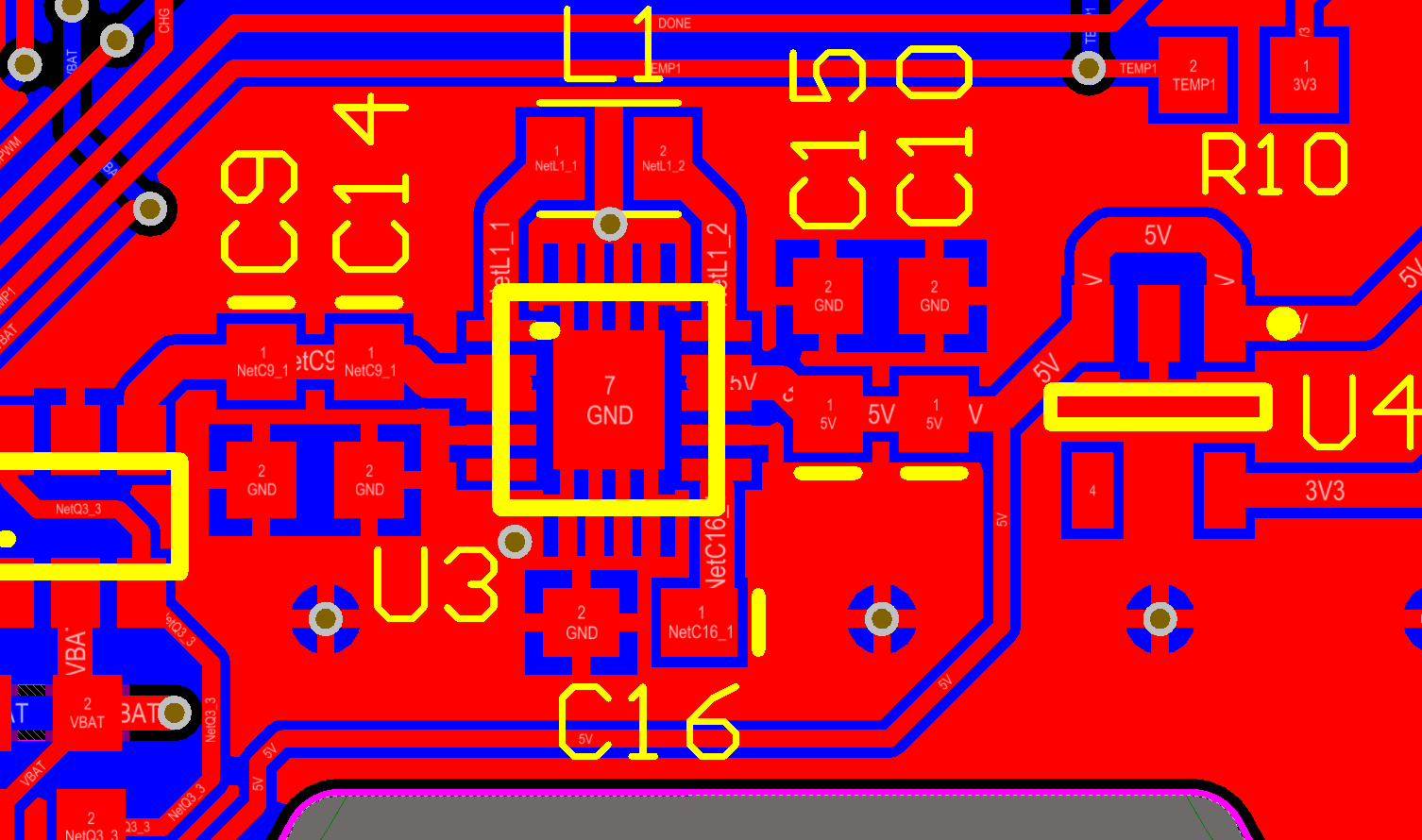
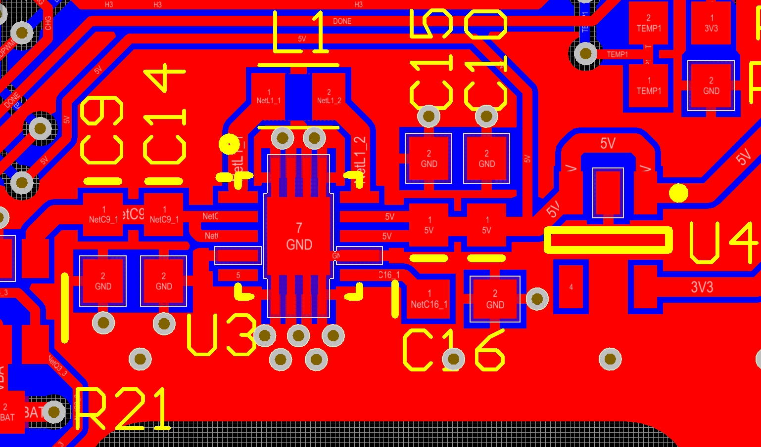
Hi! We are using this chip for battery powered application. Device has two options, either 4x AA or 8xAA battery on the input. We have realtively small batch of these devices made, all were functionally tested in house, then shipped to customers via airmail. When customers were using 4 batteries, everyhing was fine but when they used 8 batteries, device deid. Inspection showed that only thing that failed was TPS63061. Visual inspection didnt reveal anything, device doesnt look burnt, there is no shorts - no on input, no on output. 

Unfortunately we werent able to recreate the failure in house, despite vigorus attempts of overloading the chip (over voltage on input, shorts on output...) so we are really in the dark here. Also, we dont have the access to an xray machine to inspect the internals of the chip...

Any help or suggestion will be much appreciated.

  • Hi,
    Could you check if L1 or L2 is shorted to ground or VIN inside the device?
    Could you share the layout?
  • Hi,

    no, L1 or L2 are not shorted anywhere. I get aprox 2.8 Mohm from L1 or L2 to GND and even higher to Vin.

    Design with problems is this one (not much care was taken when routing this one as there were no problems with it at the time):

    We have now redesigned the layout but it has not been tested on the field yet:

    The blue layer on both designs is continous bottom side GND.

  • Hi Grega,

    thanks for sharing the layout. Indeed the first layout had a very poor ground connection (I noticed the AGND pin was not directcly connected to the powerePAD which is critical ).

    The second layout looks much better. I would suggest to add some vias under the device (as shown on the TPS63060EVM User's guide on Figure 9)
    I would also recommend to add some more vias on the ground connection of the input and output capacitor and use polygon planes for VIN and VOUT signals instead of traces.