This thread has been locked.

If you have a related question, please click the "Ask a related question" button in the top right corner. The newly created question will be automatically linked to this question.

BQ24170: Problems above 10V Adapter Voltage

Part Number: BQ24170
Other Parts Discussed in Thread: CSD25402Q3A

Buck converter of my bq24170 seems to stop working in my recent design of a battery charger (2 or 3 Cell)  if I increase input voltage above 10V (should be ok up to 17V?) 

VBat (=VSRN) is correct vor Vin < 10V (tried for 1, 4.2V and 2 8.4V). If I increase the input voltage above 10V VSRN gets switched to full VIN (resulting in high currents for 1Cell) 

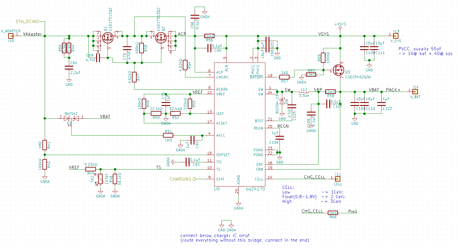
Vref is 3V3, VREGN is 6.0V (clean)

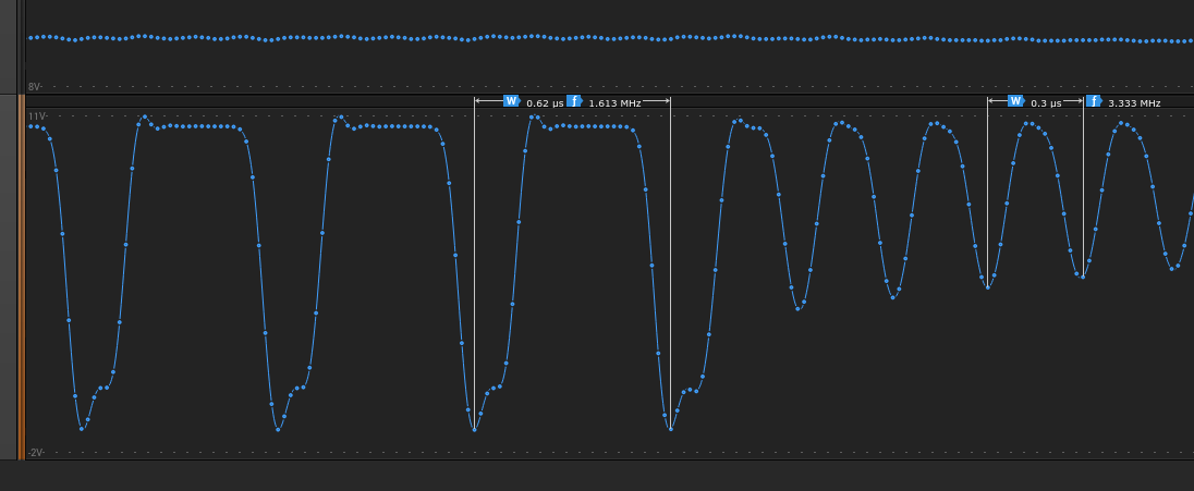
ACDRV (ca 4-17V   @ ca 13V Adapter Voltage): 

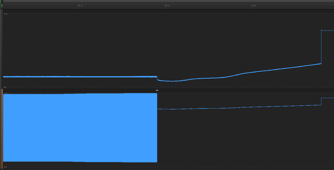
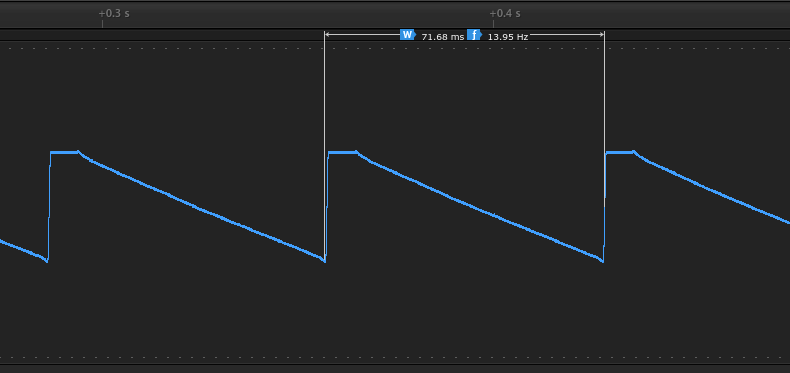
VSRN (11-12V @12V Vin)

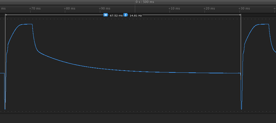
measurements without load ( system input capacitance ~ 40uF which I tried to remove -> no difference)

with VIN = 9.5V I get Vsrn 4.2V (with and without load) 

any help appreciated

  • looked some further

    2 Cell charging while increasing Vin from about 10V to 12V produces following VBat and SW graphs (top: VBat 8.4V until Vin > ~11.5V afterwards rises to VIN): 

    same graph zoomed in: 

    with increasing Vin the voltage curve of SW reaches negative values. Is this normal? should that be the case? 

    no load (same graphs)

    working sw curve:

    just before it stops working curve looks like:

  • Tried increase and decrease Cout, Cin, ...  nothing seemed to make a difference.

    Removing BatFET seemed to solve the issue. (even running off battery works via diode within charger?)

    I am using CSD25402Q3A instead of CSD25401Q3 (difference looks to be marginal?) 

    am I missing something? 

  • Andreas,

    Make sure that the drain and source of the CSD25402Q3A is connected properly (or soldered properly), where the body diode is connected so that it is blocking the system voltage, only allowing path from battery to system.

    Regards,
    Steven
  • Hi Steven,

    thanks for your answer. I am not sure that this is the problem as gate line gets weird signals as well. Also I have the same behavior on both boards I tested and the board was soldered using a reflow oven. 

    Could my layout trigger that problem? 

    unfortunately I did not follow the layout guideline #2. As you can see in the screenshot I have 2 vias for SW terminals, a wide trace via the B220A-13-F via and 4 more vias going back up to the inductor. So not optimal. Could that cause the misbehaving of the charger? 

    I just ordered new pcb with better layout to see if that solved the problem. 

  • Make sure the power traces are not going through vias (or minimize the use of vias as much as possible). The high power paths need to be optimized so that the converter can work properly. Input caps should be close to PVCC, output caps close to sense resistor and inductor. The path between the inductor and SW should be wide and short. The schottky diode on SW should be close to the pin.

    Regards,
    Steven