This thread has been locked.

If you have a related question, please click the "Ask a related question" button in the top right corner. The newly created question will be automatically linked to this question.

LM5050-1: LM5050-1 application issue

Part Number: LM5050-1

Hi Team,

My customer is using our LM5050-1 as Oring in the new project. Below is the schematic:


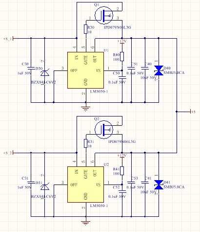
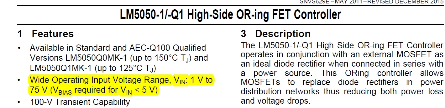
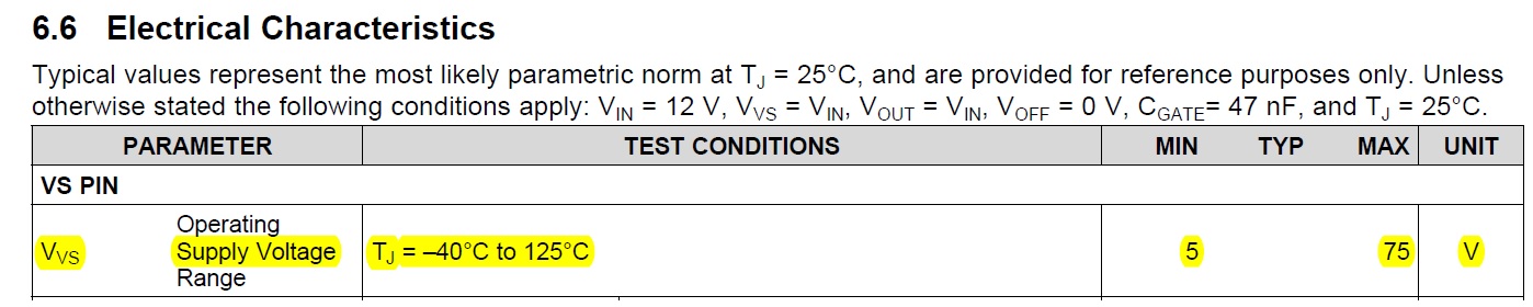
As you can see, both the master and slave supply is 5V. The VS supply for each LM5050-1 is 12V but not 5V, thus will make sure the VS supply meet the required electronic Characteristics showed in datasheet and I listed as below even when input supply voltage may a little bit low than 5V:

However, during customer's test under -40C, the output waveform is abnormal, like below:

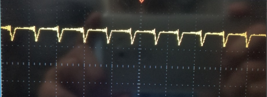
Can you help check any reason may cause this abnormal output waveform? Thanks a lot for the support!

Best regards,

Sulyn

  • Hello Sulyn
    Thank you for posting the question.
    I am looking into this, let me get back by tomorrow.
    Regards
    Kari.
  • Hi Selvaraj,
    Thanks for the support! It's urgent for customer because they need to do certification very soon.
    BTW, based on more test, I want to let you know one more test result. If we add one more 10W electronic load(Totally about 20W, 10W board load + 10W Electronic Load), then these is no such abnormal waveform. We didn't change anything except add a 10W electronic load. Hope this helps for you analysis, thanks a lot!

    Best regards,
    Sulyn
  • Hi Sulyn,

    At less load (10W), gate voltage is possibly close to FET turn on voltage and oscillates.

    This causes the FET to turn ON and OFF.

    Could you please share the complete waveforms of two inputs(5V master and slave) and the gate voltages of the two MOSFETs.

    Regards,

    Kari.