Other Parts Discussed in Thread: UC2825B, UC2825A
Hi
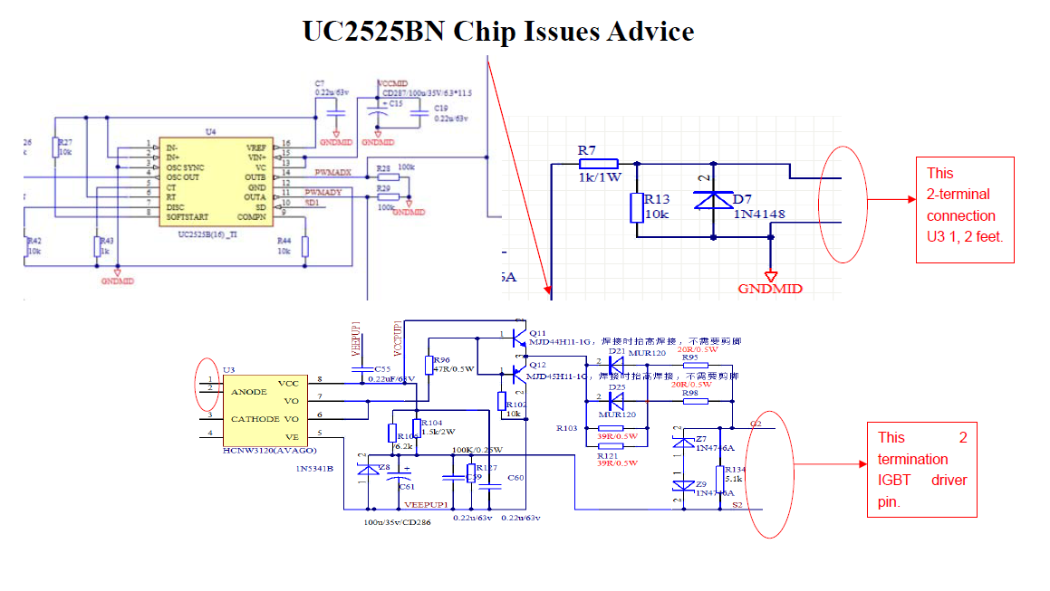
My customer has some query with UC2525BN.
whether this circuit design has any adverse effect on the UC2525BN. Or long run to reduce the service life of the chip? Above the circuit design above whether there are flaws? The current problems are
as follows:
1, G2, S2 drive without drive waveform.
1.1 After checking the PCBA board found Z7, Z9 has been burned, the function fails. The most serious degree is: the middle of the regulator directly
broken. After the replacement after Z7, Z9 drive normal operation.
1.2, another kind of situation, when G2, S2 without waveform, check Z7, Z9 also without damage, the function is also invalid. In view of this, we directly
replace the UC2525BN chip, the final drive-side normal.
NOTE:By calculating how to judge this circuit design flaws? Very much hope that your company's engineers answer, in this very grateful.
Thanks
Star


