This thread has been locked.

If you have a related question, please click the "Ask a related question" button in the top right corner. The newly created question will be automatically linked to this question.

BQ34Z100-G1: Communication logic not in common GND?

Part Number: BQ34Z100-G1

Hello there,

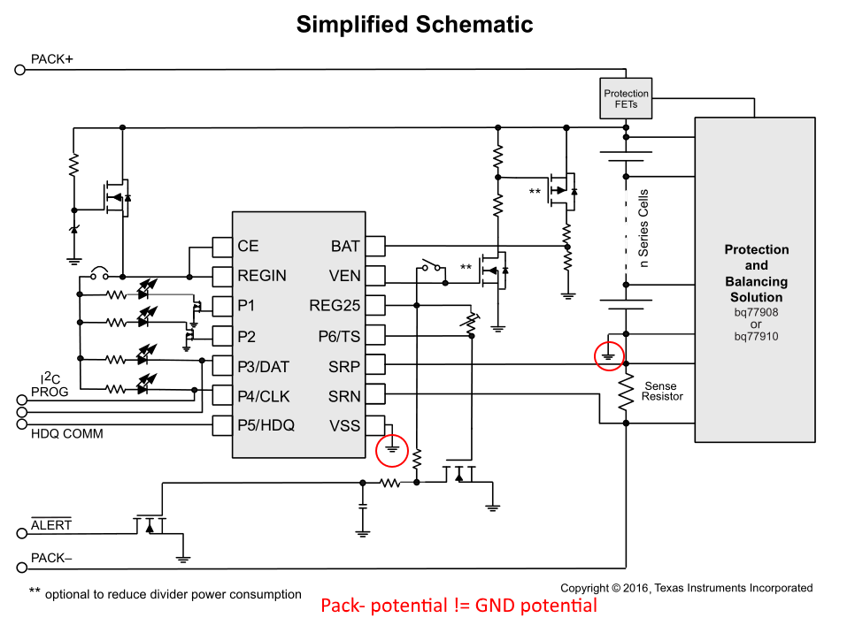
I am currently designing a board featuring the bq34z100-G1 device. Looking at the application note I am hacing some doubts either I understand everything correctly. Please take a look at the bellow figure from the datsheet:

As you can see above, the device GND will not be equal to the other circuitry GND connected through PACK+ and PACK-. In means of communication through I2C can cause trouble, since the external driver will pull to its own GND, and BQ will pull to the local one. The difference between grounds would be the voltage drop across R_sense.

Is this by design? I would really appreciate additional explanation, I need to move on with the design.

PS: I have noticed some inconsistency: The pinout table states that VEN is an OUTPUT, whereas from the description it seems as its an INPUT. Is this an error?

  • Hi Lukasz,

    For full scale current sensing, the differential voltage between SRN and SRP is specified to be +/- 125 mV.  Please size your sense resistor so your maximum current does not cause a voltage drop across the sense resistor in excess of +/- 125 mV.  With the maximum offset limited by your design, for i2C communications where bat - is referenced as ground, low/high threshold ranges of Vcc * 0.3 V / Vcc * 0.7 V, respectively, will still be met.

    VEN is an output. It is used to turn on/off the external voltage divider illustrated above (the divider network connected to the BAT pin). This is to save energy that would otherwise be sunk through the resistor network when the resistor network is not being measured. I agree, the designation VEN is a bit confusing, as it usually stands for Voltage Enable in many other parts. For the bq34z100-G1, VEN stands for Active High Voltage Translation Enable. Perhaps AHVTEN wasn't catchy enough? In any case, thank you for the feedback, I will pass it on to our systems team.

    I hope this explanation clears these two issues up. If you have any other questions, please let me know!

    Sincerely,
    Bryan Kahler

  • Hello Bryan, thank you for answer.

    I do not fully follow your explanation regarding the ground levels. If I understand correctly, the PACK- terminal is the ground level of all external circuitry. Now lets consider the I2C bus. Lets say the SDA/SCL lines are pulled up via resistors to a 3V3 voltage source. At this point a question arises, isnt there any voltage level translation needed on the SDA/SCL lines, since the digital logic of the BQ chip is 2.5V? But the datasheet says from -0.3 V to 5.5 V so lets say this is less of a problem. What I am wondering more about is the situation when the SDA/SCL open-drain outputs are turned on. Lets say the MCU is querying something on I2C line from the BQ/ He pulls the SDA/SCL lines low, and hes "low" level is the PACK- level. In this case he is going under the GND level of BQ (by the voltage drop across the R_sense). Is that why in an example schematic protection diodes are added?

    As for the VEN PIN, please take a look at the above schematic. It is definitely used an input (REG25 is an output). Also reading the datasheet (Page 38):

    "The button applies 2.5 V from REG25 pin 7 to VEN pin 2 (refer to Typical Applications)."


    How is this not an input?

    I would appreciate further help.

  • Hi Lukasz,

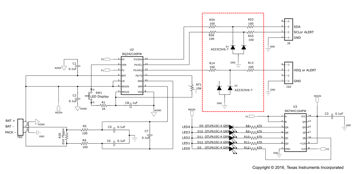
    The primary use of the protection diodes is for protection against overvoltage/transients. As you pointed out, the pins are tolerant up to -0.3 V, more then double that of the max negative drop across the current sense resistor.

    Thank you for the discussion with respect to VEN. It is primarily used as an output, but is connected to the GPIO block as illustrated in the block diagram of the Datasheet. I have passed your feedback on the systems teams.

    Sincerely,
    Bryan Kahler

  • Thank you for answer,

    So can you confirm that the voltage level difference (of R_sense drop amplitude) on the signal lines (SDA and SCL) is intended by design, and in order to handle this properly shunt diodes are needed?

  • Hi Lukasz,

    If using the bq34z100-G1 EVM, GND is referenced to Bat-. You may reference GND to PACK-, however, please modify the GNDSEL bit in the Pack Cfg register.

    You may also reference the device and its external support components to BAT- and the I2C bus to Pack-. The voltage drop across the sense resistor will not be large enough to cause communication issues.

    If you have any other questions with respect to this, please upload a schematic of your design so the discussion is not being held in the air. Thank you!

    Sincerely,
    Bryan Kahler
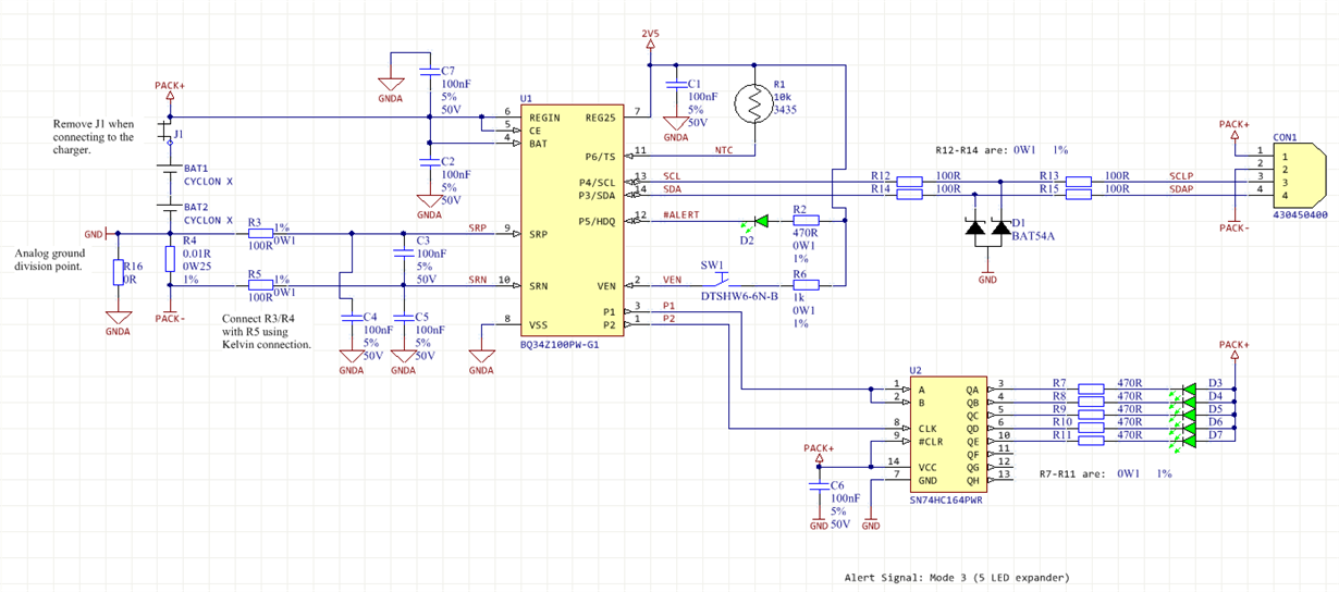
  • Here is the schematic:

    The ground reference is really not about the BQ chip, but the external devices communicating on I2C. As you can see on the schematic the external device will reference to pack-, the BQ references to PACK- and voltage drop across R_sense (local GND). Each time the external device will drive the open dair io (SDA and SCL) the D1 diodes will conduct. This isnt normal behavior.

    PS: The application should work with 2 serial Lead-Acid cells (Total voltage from 3 to around 4.5 V).

  • Hi Lukasz,

    With respect to ground, the basic rule is:
    1. If the signal does not connect to anything external to the cells and gauge i.e. the system, load or charger, then it gets referenced to Vss.
    2. If the signal goes to the system, load or charger, the it is referenced to PGND/PACK-

    Sincerely,
    Bryan Kahler