This thread has been locked.

If you have a related question, please click the "Ask a related question" button in the top right corner. The newly created question will be automatically linked to this question.

BQ24250: Increase load current from 2A to 4A with an external bypass diode?

Part Number: BQ24250
Other Parts Discussed in Thread: BQ24190, BQ25606, BQ25601, BQ25895

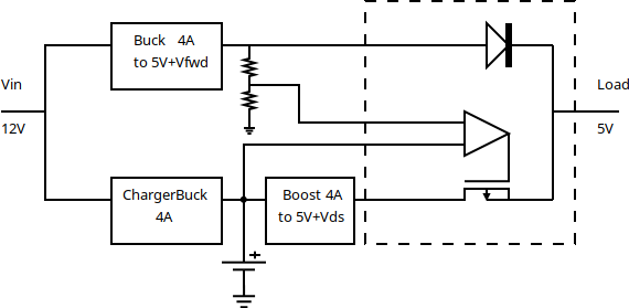
I have a load that might draw up to 4A. I want to power this load either from battery when no DC is available, and from DC IN when it is available. While the load is powered, I want the battery to charge at a high charge current 1.5A or 2.0A).

From my reading of the datasheet:
maximum discharge current from battery to load: 4A [good news]
maximum input current to Vin: 2A [bad news]

Will the following work? And specifically, will the BQ charge the battery at full charge current? My reasoning is that it will because D1 will prevent SYS from ever drooping, even when the load pulls more than the 2A limit of the BQ, correct?

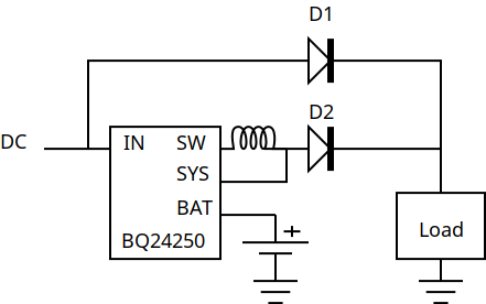
My rationale for D2 is that otherwise D1 will create a path from DC IN to BAT (via internal FET between SYS and BAT, when that FET is on), which does not seem right.

  • The bq24250  is a narrow VDC (NVDC) charger with power path. The integrated power path is the feature that you want to implement. You don't need either D1 or D2. Please refer to the figure below. The current path 1 is one directional and has higher priority. The current path 2 is bidirectional to charge the battery or supplement the load current if the DC source is absent or the power not enough.  

    For your application, the standalone bq25606 or I2C controlled bq25601, bq24190 are good options as well.  

  • Thank you for your response. Yes, I understand that there is power-path functionality in BQ24250, and that it will work without any external diodes for currents below 2A. I am attempting to power a load of 4A while charging battery at 2A, so a total of 6A of incoming current. Will BQ24250 support 6A of current going through it?

    The datasheet says: "Absolute Maximum Ratings: Output Current (Continuous): IN: 2A, SYS,BAT: 4A. Recommended: Input current: 2A" My interpretation of this is that it can handle at most 2A while I need 6A. (Let's assume the input supply is ~5V). BQ24250 also has input current limiting functionality, with the maximum of 2A (would that limit not trip if the load tries to pull 4A?). Is my understanding of the datasheet incorrect?

    What I believe will happen if I try without external diodes, is that the BQ will power the load with 2A from the input and with another 2A from the battery: so the current into the battery will be -2A (discharging) instead of +2A (charging).

  • One problem with BQ24250 I observed is that even the basic powering from battery is not adequate for the spikes in my load, most likely due to the high Ron. (I witnessed this problem in my alternative circuit without the BQ24250, with a discrete P-FET between battery and load: unless I use a FET with a Ron<12mOhm or so, Vload droops on spikes). BQ25895 has a lower Ron of 11mOhm, so it probably won't have this issue.

    One source of my confusion was assuming 5V Vin. I know understand that I need to increase Vin such that I get enough power within the maximum input current limit. The BQ24250 is still too low current: Pin is limited to 12W and output current is still limited to 2A, so even going to Vin=9V won't help. However,  with BQ25895, despite the input limit of 3.25A, we can get the max 5A output, by setting Vin to 12V. That's sufficient for charging my application (at say 2-4A), but not sufficient for powering the load (additional 4A), so with BQ25895 my application will probably work, but the battery will charge very very slowly if load is at full power.

    Perhaps using a BQ rated for 8A  to provide a 4A to the battery and 4A to the load is an option. However, I think a better option is to dedicate a buck to the DC input and another buck to the charger, instead having one buck for both, and an external power-path OR circuit. Because with a single buck, in the DC IN mode, the circuit will buck then boost, which is unnecessary. And, the 8A IC will be hotter. In two-buck solution, the power path feature of BQ remains unused.

    I suppose the builtin power-path  feature is useful for systems with Vdd requirement of <3.5V, which can use the "merged" BQ output  from "buck OR battery" of 3.5V-4.2V directly, but not useful in systems where I need 5V, because the "merged" output still needs to be boosted to 5V. So, I am forced to boost back DC IN that was unnecessarily bucked. With an external power path circuit I avoid this inefficiency:


    Note that the OR circuit in the dashed box is available in one package IC LTC4412.
    For the charger, I'm now considering the simple charger with no built-in power path: LT3651

  • Hey Alexei,

    Based on the information you've given, I am going to suggest a simple solution that customers often use for high-current designs like yours.

    Please check out these two TI Reference Designs for a dual charger application.
    1) www.ti.com/.../TIDA-00590

    2) www.ti.com/.../PMP15011

    The difference between the two is just a device used. 2) grants the benefit of a charger that does not charge by default, giving the user the ability to choose when to initiate charging. Designers typically enable the second charger when they enter the CC region of charging.

    I would also recommend reading the following application note describing both cascaded and cascoded chargers here:
    www.ti.com/.../slyt651.pdf


    I believe this should point you in the right direction. The only thing I will note that is not present in these designs is 5V boost converter you are looking for. I would suggest looking at our power portfolio for integrated boost converters. I have narrowed down the search in my link for converters that can handle at least 4A of current, but you may need a device that can handle more.
    www.ti.com/.../products.html

    And lastly, you may already know this but if your load is a 5V, 4A load, expect to need a higher current rating at the input of the boost converter (output of the chargers).


    Regards,
    Joel H