This thread has been locked.

If you have a related question, please click the "Ask a related question" button in the top right corner. The newly created question will be automatically linked to this question.

UCC27524: Sub-synchronous rectifier based on UCC27524 easy to bad, how is it?

Part Number: UCC27524
Other Parts Discussed in Thread: UCD3138

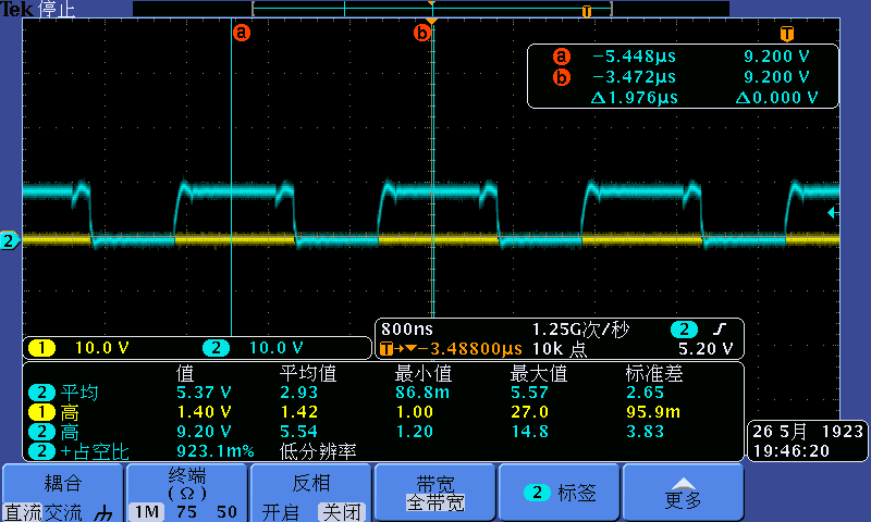
Hello, I have recently commissioned a full-bridge DC/DC power supply. Secondary with synchronous rectification, the driver is UCC27524, the drive signal input is from the controller UCD3138, the drive signal output PWM control secondary synchronous rectification MOS tube.
Now a phenomenon occurs, the drive is working normally at no-load, PWM input and output, and timing are normal. But plus light load (2A), after working for a while, the driver UCC27524 one output is broken. Change a few UCC27524, are the situation.
More depressing is that I do not know how to troubleshoot this issue, because it is not clear why the drive is broken.

  • Thanks for your interest in TI here. I've contacted the appropriate product group. You should hear from them soon.
  • Hi zoujiangyilang,

    Thanks for your inquiry about UCC27524. Sorry about the difficulty this part is experiencing in your system, I am an applications engineer working with this device and will help you out with your issue.

    From my understanding, your using 2x (or 4x?) UCC27524 to run a full bridge and at no load theres no issue however adding 2A load renders x524 output damaged...

    1. is it the HS or LS of the H-bridge driver thats damaged? is OUTA or OUTB damaged?

    a. is anything around this output damaged?

    2. are you changing anything during time of failure or is it just happening after long runtime?

    3. Are you able to capture this failure on a scope? If so, please scope INA, INB, OUTA, OUTB and VDD

    4. Can you send me a schematic of driver, FETs, load etc?

    a. what are your topology specs? Fsw, dutycycle, Vdc, etc

    Thanks

  • When doing the scope shots, we want to look for fast HF noise which could be false triggering x524 on the input and likewise overshoot or undershoot on the output. Please use short GND probe connections close to the IC.
  • Hi zoujiangyilang,

    Since we have not heard back from you this week, we must assume you've resolved your issue, so I am going to mark this thread as such.

    If you HAVEN'T solved it, please reply with the info Jeff was asking for, and we will help you resolve it.

    Happy New Year!
  • Hello, Jeff

    I tested two identical circuit boards, one UCC27524 easy to bad, the other one is good 。
    I found that easy to bad piece of UCC27524 output OUTB will have a voltage spike 15V, while the power supply is only 10V.
    Not bad piece no spikes.
    I suppose that the voltage spike of 15V burned out the OUTB, but I do not know yet exactly how this voltage spike happened, why there is one on a board, and the other one does not.

    zoujiangyilang
  • Hi zoujiangyilang,

    Thanks for your reply. If you could please send me a schematic of your driver to your fets and everything in between it would be most helpful. Any and all extra info helps. It seems, from your post I am under the assumption you are unable to provide a schematic and/or scope shots of the failure and/or any more of the questions I asked in the previous post. In that case I will have to ask other questions to paint myself a picture of what may be the root cause.

    You may very well be on to something with OUTB exceeding the max rating. It may be parasitcs but that would not explain the good board. Does the good board have any spike on it at all?

    Can you tell me when in the switching cycle does the bad spike occur? (For example right after HS turn off or LS turn on, etc.)

    What is changed from your good board to the bad board? Something must be different, is the test setup the same, with the same equipment and same test procedure?

    how many times has this happened? can you recreate this failure everytime?

    Thanks,

  • Hello Jeff.
    the UCC27524 circuit diagram on the map is to simulate your TI's UCD3138-based full-bridge hard-switching development board circuit to design. The UCC27524 driver is labeled N9 to drive the secondary synchronous rectifiers V31, V32, V33, and V34.
  • Normal circuit board OUTB waveform

  • The figure above is the waveform of OUTB on the normal circuit board.
    The slight distortion of the waveform is the moment of the primary drive PWM conversion.
  • Abnormal circuit board OUTB waveform

  • The figure above shows the waveform of OUTB on the abnormal circuit board.
    OUTB will have a spike of about 15V while the supply voltage is only 10V.
  • UCC27524 circuit layout

  • The figure above shows the layout of UCC27524.
    The 3.3VPWM driving signal from UCD3138 enters from the right side of N9 and the left side of N9 outputs 10V PWM to drive secondary synchronous rectifiers V31, V32, V33 and V34.
    The order of package pins 1 through 8 of this layout N9 is wrong.
  • UCC27524 actual assembly diagram, UCC27524 is erected welding. Its 5,6,7 feet through the wire fly to the pad.

  • Hi zoujiangyilang,

    Thanks for your update and much appreciated info! I have understood your issue. It appears that the EVM user guide http://www.ti.com/lit/ug/sluua95/sluua95.pdf figure 32 shows the switching waveform of the powerstage. The spikes like you said are due to primary side. Since this spike lines up with the master leg switch node (TP23) then as the master HS fet of the primary full bridge turns on the switch node experiences a ringing due to the parasitic inductance and LS fet parasitic capacitance on this node forming a LC resonance. The resonance spike will become magnetically induced through the core and coupled to the transformer secondary and manifests itself as a spike on OUTA in the EVM userguide (however I understand its OUTB in your case...maybe they are just swapped...to confirm your scopeshot, the SR FET is ON when the spike occurs is the fet being damaged). You can read about this ringing phenomenon in this AN - http://www.ti.com/lit/an/slyt465/slyt465.pdf. You have a few options to reduce this ringing spike. The following 2 will aim to reduce the magnitude of the ring: Add a gate resistor to slow down the HS fet and therefore the high slew rate on SW. Add Rboot for a similar effect. The 3rd method is for dampening the frequency of the ringing with a snubber with a lesser affect on magnitude.

    Anyhow, Let me reachout to the controller team and get their input as well. I will update you with their reply tomorrow.

    Thanks,

  • In the mean time i will take a closer look at your layout, also I believe the quick fix would be to slap a zener on it and clamp OUTB to ~10V. And If possible, I would like to see a scopeshot of the master leg SWnode to see if this is really where the spike is coming from.
  • Hi zoujiangyilang,

    Update: still awaiting controller team's reply. From what I can see on this top layer, layout is not bad. Are you using the blue wire on both good and bad boards? do you think this issue could this issue be due to soldering?

    Thanks for your patience,
  • Hi zoujiangyilang,

    After talking to the controller team my previous post sums up their reply. Any update with this issue?


    Thanks,