This thread has been locked.

If you have a related question, please click the "Ask a related question" button in the top right corner. The newly created question will be automatically linked to this question.

UCD3138HSFBEVM-029: UCD3138 PWM drive capacity is not enough

Part Number: UCD3138HSFBEVM-029
Other Parts Discussed in Thread: UCD3138, UCC27524

Hello, I am simulating the UCD3138 full-bridge hard-switching evaluation board to make a DC/DC power supply. I encountered some problems.


The first question:

The UCD3138 PWM0A signal into the digital isolator ISO7140 INB and IND pin, the level will be reduced from 3.3V to 1.2V, and if PWM0A only enter a pin IND , the level remains 3.3V. I tested the development board,  PWM0A  can drive 2 digital isolator in development board, but My  power supply can not.

The second question:

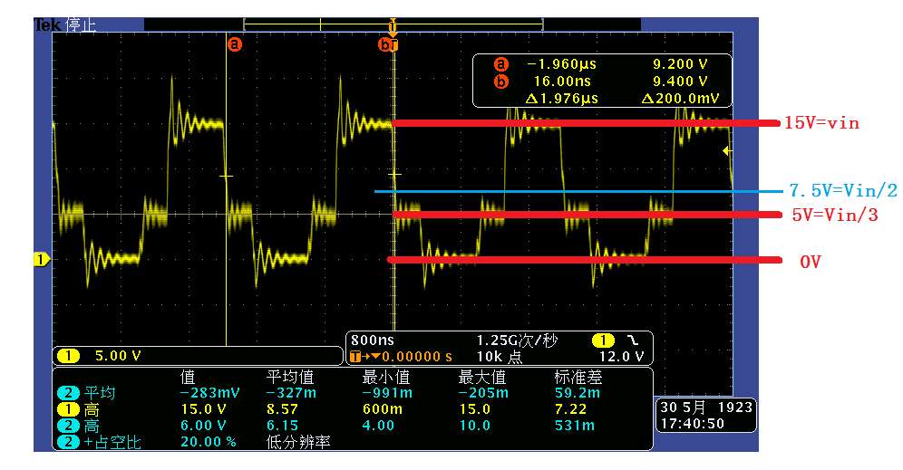
Development board transformer primary winding TP23 or TP25 waveform is 0V, Vin / 2, Vin to change. And I do the experiment board is 0V, Vin / 3, Vin to change.  I put the 5k Ohm resistors in parallel with the DS poles of the four primary MOSFETs,but  the waveform is still 0V, Vin / 3, Vin to change.

The third question:

My experimental board secondary synchronous rectification driver UCC27524 OUTB pin to work for some time, it is broken, there is no output. I tested the pin, the pin will work when there is a 15V spike, excuse me, is this 15V spike OUTB broken it? What is the withstand voltage of OUTB? I did not find it in the UCC27524 manual.

  • On the first question, the ISO7140 only requires 10 μA to pull it high or low, so I don't think it's a drive strength issue. It sounds to me like the INB pin is also attached to some other output which is trying to pull it low.

    I don't understand the second question. Especially, I don't understand how it is a device question. Can you provide some more detail? Is the UCD putting out the correct waveform to drive the power supply?

    On the third question, the spec for OUTB is dependent on the supply voltage to the UCC27524. So if the supply voltage is 15 V or above, you are OK. However, if the supply voltage is more than .3 V below 15 V, there is a risk of damage.
  • Hello lan Bower,

    Thank you for your reply, your guidance let me realized it suddenly!

    For the first question, I think your statement is correct. When I used DPWM0A to drive the INB and IND of the ISO7140 , the INB pin was connected to the DPWM2B at the same time, and the DPWM2B did not work. I think as you said, the DPWM2B pin is pulled low. Thank you.

    For the third question, I now have two identical power supply, one of the UCC27524 OUTB vulnerable,but the other one is good. I compared the two waveforms and found that at a supply voltage of 10V, the bad one OUTB had a voltage spike of 15V, but the good one had no spikes. I suppose that the 15V spike breaks outbudding OUTB, but I do not know yet exactly how that spike was generated.why one is on the circuit board and the other is not.

    Thanks

    zoujiangyilang
  • Hello lan Bower,

    For the second question, see the above waveform.
    The figure above is the transformer primary voltage waveform to earth, similar to UCD3138 development board No. 29 TP23 or TP25 waveform. When the input voltage is 15V, the platform voltage is about 5V instead of the ideal 7.5V.
    I am very confused. I changed the MOS, the DS side of the MOS in parallel with the same resistance, found no use.
    I tried to overload the MOS side of the DS-side parallel 10000pF capacitor, the platform voltage can reach the ideal 7.5V, but this way, the efficiency will decline.
    I want to know why the platform voltage, not the ideal Vin / 2, is the difference of the stray capacitance of the circuit board, resulting in the equivalent capacitance of the upper tube DS and the lower tube DS ?
    in addition to parallel 10000pF capacitor, are there other ways to solve the problem and not reduce efficiency?

    Thank you
    zoujiangyilang