Other Parts Discussed in Thread: TPS3710
Hi,
The LMZ34002 is used to generate -5V@1.6A from 12V input supply.Switching frequency is chosen as the 500KHz, the soft start of 10ms and UVLO=6.5V.
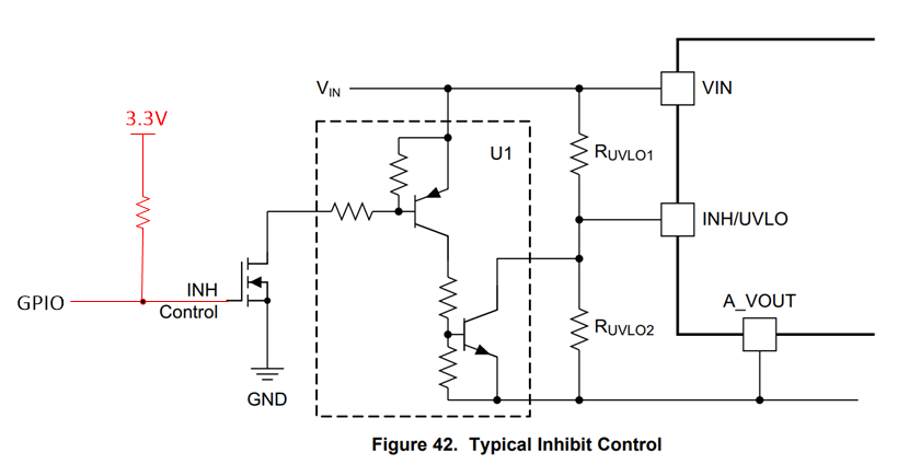
As per the project requirement, LMZ34002 should be Power-ON with outputs disabled. The schematic on the page:21 is exactly opposite to our requirement.
From the datasheet it is well understood that INH/UVLO pin can't drive directly, some level shifting mechanism has to be used.
Here, INH/UVLO pin has to be controlled (indirectly) from GPIO of uC/FPGA.
I can't ensure that this GPIO will be at Ground during initial Power-ON or during reset.It can be at High-impedance during initial Power-ON or during reset.
But LMZ34002 output should remain disabled until GPIO of uC/FPGA is driven high(3.3V). Then only we can implement proper power-ON sequencing.
Q1. Please suggest a mechanism to implement the above requirement?
Please find the attached image that implements the above requirement with DCX144EH-7 and TPS3710.
But it may give glitch at the output during power ON due to the following reason.
The OUT pin of TPS3710 is at undetermined state until VDD ramp above 1.8V plus 150micro second delay. So it can turn OFF the PNP transistor associated with DCX144EH-7, thus turning ON LMZ34002.
Q2. DO this problem result in glitch at the output during Initial Power-ON? How to solve this issue?Please have a look at attached image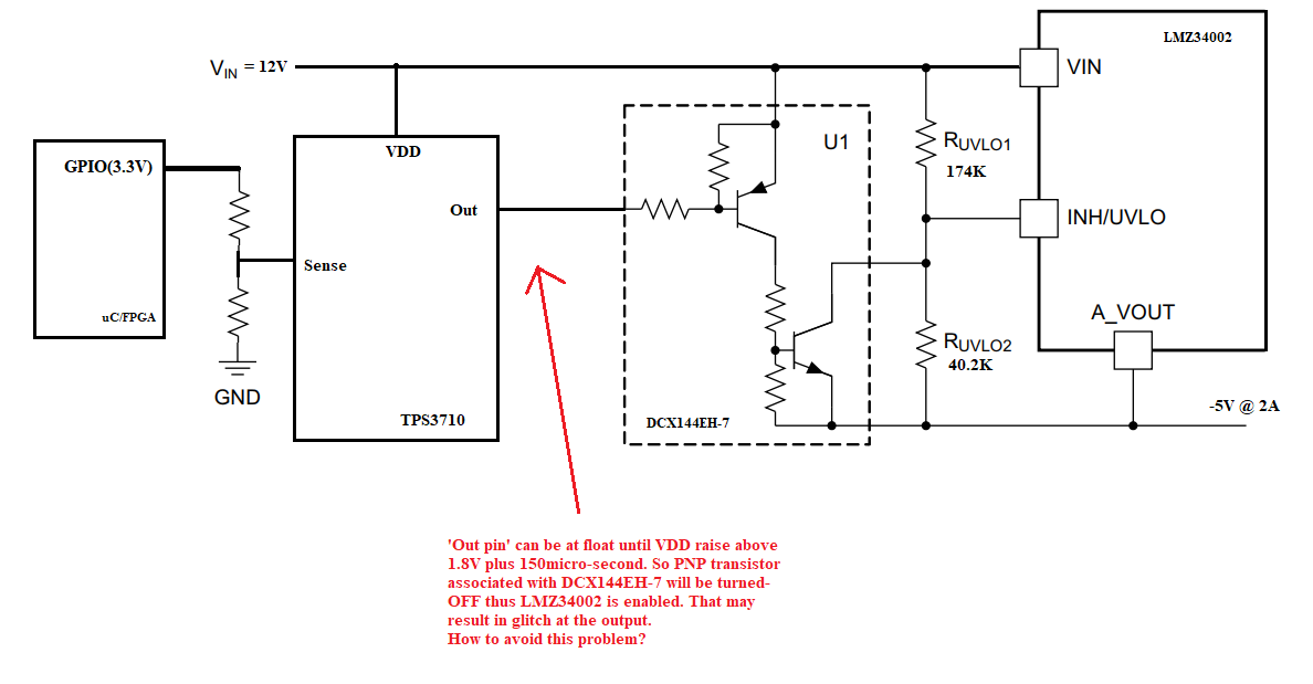
Thanks in advance
DEEPAK V