This thread has been locked.

If you have a related question, please click the "Ask a related question" button in the top right corner. The newly created question will be automatically linked to this question.

UCC28C45: Gate driver IC with negative turn off bias

Part Number: UCC28C45
Other Parts Discussed in Thread: UCC5310

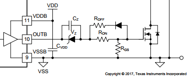
Hi, do TI produce a gate driver IC with negative turn off capability without the need for a negative rail? I'd rather avoid gate drive transformers if possible so maybe a device using some kind of charge pump?

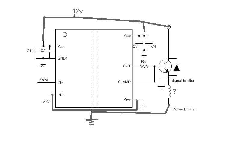
I ask as I have a problem with capacitive coupling turning the fet back on in my flyback supply, the spikes are caused by the drain to gate capacitance of the sihg73n60e mosfet. The gate drive voltage is 12v and the short spikes on the gate are only a few volts max but the turn on threshold for this fet is 2v minimum so it does cause it to turn back on slightly, I have a 2.2k pulldown resistor and 18v zener on the gate but that does nothing since the spikes are positive with respect to the source pin. Putting a turn off diode across the 12 ohm gate resistor fixes it but causes other problems due to dv/dt.

So I'm thinking +/- gate drive might be the way to go since I can't have the gate turn off too fast via a diode or other low impedance discharge path, going negative at turn off would allow the drain to gate capacitive coupling to still occur but since the gate will be negative it wouldn't allow the fet to turn back on,

Do Ti produce such a device that could go between the UCC28C45 and MOSFET? It would need to somehow produce the negative voltage swing from a single 12v rail and be able to run at 20khz, non isolated is fine and the N channel fet is on the low side.

Thanks.

  • Hi John,

    Thanks for using UCC28C45, I am an applications engineer working with high power gate drivers team that should be able to help out this issue and any other questions you may have.

    Without a bipolar supply or isolation needed, its possible to sink miller current using a unipolar supply and the active miller clamp protection featured option on our UCC53xxM parts (UCC5310M and UCC5350M). With the UCC5310M being the most suitable for your application.

    At the turn on miller plateau the Cgd (miller cap) goes from having high voltage (Vout or Vin for example) at the drain (seeing small Cgd – C=Q/V so bigger voltage means smaller capacitance) to having ~0V at the drain (seeing larger Cgd) and similarly at turn off the drain goes from 0V to Vout or Vin making it look smaller (with faster time constant) and if this dv/dt (caused by a high voltage slew rate transition on drain) happens too fast then there will be a fast discharge in the direction of the voltage drop during the plateau manifesting a spike on Vgs because this parasitic turn on current has nowhere to go.

    This protection feature operates as follows:

    The Miller clamping function is implemented by adding a low impedance path between the gate of the power device and VEE2 supply. When the switch is turned-off and the gate voltage transitions below 2-V the CLAMP current output is activated. Miller current can sink and the gate voltage is clamped to be lower than the turn-on threshold value for the gate. To prevent the switch to turn on, the CLAMP pin is connected to gate and Miller current is sunk through a low impedance CLAMP transistor. Miller CLAMP is designed for Miller current up to 2-A. The ‘Active output pulldown feature’ ensures that the gate is clamped to VEE2 to ensure safe off-state, when the output side is not connected to the power supply.

    Please let me know if you have any more questions.

    Thanks,

  • Thanks for the technical advice and recommendation. Wow that's a really neat little driver IC, will see if we can get some ordered in for testing.

    What's the difference between the UCC5310M and UCC5350M? Is it just peak drive current capability?
  • Hi John,

    I know, its an amazingly elegant solution for a feature packed power FET and IGBT iso driver!

    Thanks for your follow up, great question because at first glance the performance is the same except for the drive current. Of course this means the Rds_on of the HS totem pole NMOS is lower for the 5350 for higher current draw likewise the paralleling of the miller FET (Rclamp) and LS totem pole NMOS equates to lower resistance for the respective output section in which the 5350’s Rclamp is less to sink more current.

    But I took a closer look and there are some differences. I first went to TI.com clicked on UCC5310 product page and scrolled down a bit to compare all our UCC isolated gate drivers. The difference from here says the max prop delay is 75ns for 5310 and 100ns for 5350 (the typical prop delay is 60ns – 5ns smaller than 5350). The ds supports this. Over-all they have more or less the same functionality.

    Thanks,
  • Thanks! Is it ok for the input and output sides to share the same 12v supply? In other words I will be defeating the isolation with VCC1 and VCC2, Ground1 and VEE2 connected respectively.

    Or will this cause problems? This schematic shows how I plan on using it.

    Also what is that inductor in the emitter path? Is it just parasitic inductance or an actual inductor/primary coil? If so does it matter that mine is above the fet between +12v and drain.

    Edit: another question, what is the max voltage allowed on the PWM "in+" pin? As the PWM IC will be putting out 12v max.

  • Hate to bump this thread but would my schematic below 100% work? The PWM in signal will also be +12v ground referenced to both rails.
  • Hi John,

    Thanks for your follow up and helpful circuit layout. Sorry not being able to reply sooner.

    You guessed it. There is no issue with defeating the isolation. Vcc1 and Vcc2 can be powered from the same supply and 12V falls in both ranges. The input logic thresholds are both the same and are dependent on Vcc1. The abs max input threshold voltage is Vcc1+0.3. So a 12V PWM signal does not leave very much headroom. (note: The inductor represents is a model for line inductance that is integral to this IGBT design).

    There is another option that may be cheaper if your application doesn't include a variable dutycycle. My teammate has brought this to my attention which he will reply on this thread soon after this post with the details of this negative bias with positive rail discrete circuit solution.

    In the mean time feel free to ask any more questions and I will make my best effort to answer them before the end of the day.

    Thanks,

  • Once again thanks Jeff for answering all my questions!

    How about a regular diode between the common +12v rail and UCC28C45 Vdd pin? That would give .7v more headroom and if close attention is payed to the PWM input line then any ringing could be minimized to prevent overshoot into the red zone. Its the same +12v rail so it *should* be more or less at the same potential excluding parasitics.

    Or a potential divider on the UCC28C45 output pin?


    The design does use duty cycle control to limit the current, max is 50% but does go all the way to 0% since its also doubling as a way for the user to control load power (its a bit of a specialty product). I would however be interested in seeing what your teammate has come up with as maybe I could find a way to implement it.

    Thanks.

    J

  • Hi John,

    I work with Jeff in on the gate drivers team. I saw that you were trying to generate a negative bias from a single supply, and there is a circuit which can do that using a zener diode and a capacitor. See the image below:

    I was going to suggest this as a possibility, but based on your recent comment I think it will not work well at lower flyback load current since the negative biasing starts to diminish with duty cycles below 50%. Additionally, since the circuit only shifts the peak to peak output down by the nominal zener voltage, the VDD biasing would have to increase to support this (e.g. for +12V/-5V biasing, VDD=17V). If you are still interested, I can provide a more detailed description. But it sounds like the miller clamp solution would work just as well, and would likely require fewer changes.

    Regards,

  • Thanks Derek! Wow that's quite an elegant solution. I would definitely be interested in the more detailed description, but as far as I can tell the capacitor remains charged to the zener voltage which then appears in series with the gate as the output pin goes low and the gate discharges.

    Does a larger Cz also slow down the gate rise and fall times and what kind of capacitance is a good starting point? I guess it needs to be just large enough to last the off cycle or at-least to the point where the miller induced pulses appear.

    I think what I'll do is give Derek's suggestion a try first as giving our UCC28C45 a few more volts would be easy and the miller induced gate spikes do seem to diminish with less primary current, so maybe the duty cycle dependency would't matter as much.

    Then if it turns out not to work in our application we'll go with Jeffery's original suggestion of the UCC5310M or UCC5350M.

    Thanks again to you both.
  • Hi John,

    I think you've intuited basically how the circuit behaves. A zener diode is used to set the amount of negative bias. After several cycles, the capacitor Cz will develop a voltage across it, clamped by the zener reverse voltage, and the output waveform will be shifted down by the voltage on Cz. To your question about rise and fall times, Cz and Rgs behave like a high pass filter with a corner frequency that is usually much lower than the frequency of operation, so rise and fall time are rarely impacted by this circuit.

    To give you an example, I simulated a circuit with 17V output supply, 22nF load (about 380nC at 17V, based on SIHG73N60E datasheet), Cz = 1µF, and a 5.1V zener diode (1N4733A/PS, with 49mA test current for 5.1V). The results of a 20kHz, 50% duty cycle simulation are in the image below. You should be able to see that the voltage across the 22nF load capacitor (graphed) gradually drifts down in voltage until it reaches some stable negative bias on the output.

    There are a few details to operating this negative bias circuit properly:

    • The initial turn-off value of the circuit is primarily determined by the ratio of Cz to the load capacitance. In the image above, Cz is 1µF and the load capacitance CL is 22nF, so the initial turn-off value is 17V * 22nF / (22nF + 1000nF) = 0.365V. This suggests that a larger value of Cz is beneficial during startup, to keep the initial turn-off voltage near 0V.
    • The quiescent current for the zener biasing is determined by the zener voltage at steady state, the duty cycle, and Rgs. I simulated for 1N4733A/PS, with a 2.2kΩ Rgs and 8.5V supply (17V at 50% duty cycle), Vz = 4.787V and Iz = 1.688mA. These values make sense for a 5.1V zener well below test current. Note that the zener biasing current isn't the full quiescent current added by the circuit, which is hard to predict without simulation.
    • The final turn-off value of the circuit (at sufficient duty cycles to permit it) is primarily determined by the zener voltage at our calculated Iz, and the ratio of Cz to CL. In the example waveform, the zener voltage declines to -Vz + 0.365 = about -4.422V.
    • The time before the negative bias reaches its "steady state" as it transitions from one duty cycle to another, is primarily determined by the value selection of Rgs and Cz, and the duty cycle. In general, smaller Cz and smaller Rgs allow Cz to charge to its steady state value faster. In general, as positive duty cycle increases, the average quiescent current through Cz and Rgs increases, and the bias voltage is reached faster.
    • At low duty cycle, there is some impact on steady state reverse bias due to Cz being discharged through Rgs during turn-off. Charging during on time and discharging during off time reach an equilibrium point where the negative bias voltage will be less than the zener diode voltage. There also seems to be an opposite effect where higher supply voltages at the same low duty cycles shift the equilibrium point to a lower negative bias.

    Given the number of contributing effects, I am still studying aspects of this circuit to reach a numerically driven approximation, especially for settling time and steady state negative bias. My recommendation is to put the duty cycle, supply voltage, and Cz/Rgs/Vz combination of interest into your favorite SPICE simulator. This will give you the most accurate behavioral picture.

    Best regards,

  • I can't thank you guys enough for the help you've given me in this thread! I'm sure it'll also help many other lost souls searching the forum for similar answers.

    Derek I'll be giving this a try in the week and hopefully either this or the miller clamp IC's will allow us to fix this and focus on other areas. I think it all boils down to the sihg73n60e being a heavy MOSFET to drive, problem is we need that high D-S voltage rating and low on resistance.

    Thanks again!
  • Looks like I've hit a snag with the recommended IC's, they have a UVLO of 13.8v when we're using 12v.

    In other news whilst experimenting I've come across something-else that helps, a single capacitor across the gate resistor (gate to PWM output) reduces this miller spike by a good margin. Right now I'm at 10nF and can probably go lower, it does reduce switching speeds somewhat but at this point not by much.

    I can't find any references to this practice online so that leaves me wondering if its bad practice. I guess it just AC couples that miller spike to ground.

    Has anyone come across this practice before? The 10nF capacitor is across the gate resistor between the PWM output pin and MOSFET gate.

    Edit: Looks like 10nF is the sweet spot. Its a far cry from a miller clamp or negative drive bias and I wouldn't say its solved all my issues, but its still interesting.

  • Hi John,

    What you are describing sounds like a speed-up capacitor, a classic circuit for accelerating transistor turn-on and turn-off. I have seen it more commonly in BJT switching applications, since it is useful for rapidly extracting the stored base charge that accumulates during saturation. Although I have heard no specific mention of speed-up capacitors as a bad practice for FET-based circuits, I think this is because the advantages of a speed-up capacitor can be realized in a way that does not undermine the use of a gate resistor. Adequately sizing the speed-up capacitor can be puzzling: too little capacitance forms an AC voltage divider with the FET input capacitance, limiting Vgs swing; too much capacitance is equivalent to shorting the gate resistor, and this risks damaging both the FET and the driver with ringing (especially with modern high current gate drivers). In hard-switching applications, the Miller plateau gate charge will pass through and charge up the speed-up capacitor, further limiting Vgs swing. And a speed-up capacitor cannot easily be exclusively applied to turn-on or turn-off, since a capacitor in series with a diode creates a peak detector. In most FET-based circuits it would be simpler just to set Rg = 0Ω.

    The reduction in the miller spike is because, when the gate driver output is low, the speed-up capacitance Csp is put in parallel with the existing Cgs. Since ΔVgs = Δt * I / (Cgs + Csp), and since roughly same dv/dt-induced current flows through the drain-gate and gate-source paths, the voltage which appears from gate to source is substantially smaller than the one which appears from gate to drain, effectively flattening the miller spike. The same effect could be achieved by adding an external capacitance from gate to source of the FET, at the cost of some switching speed and additional power dissipation.

    Regards,