


Other Parts Discussed in Thread: TPS1H100-Q1
Hi Team,
Good morning, one of my customers is using the TPS2H160-Q1 in their design and when using the 1k resistor in parallel with a 1N4148W diode, the input voltage relative to ground is exceeding the rating of -0.3V. With this, how should they implement the reverse voltage protection scheme where an MCU is intended to connect the input pins to ground without violating the abs max rating?
More info from the customer -----------
We are using the TPS2H160BQPWPRQ1 in a current design and have discovered a couple issues when installing the reverse polarity protection diode and resistor pair at ground. Our circuit snippet is as follows:
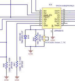
We are using the reverse current protection in Figure 25 of the datasheet.
First, we initially used a 1k resistor in parallel with a 1N4148W diode. The 1k is sugested on the datasheet, page 23. We observe a forward voltage of 0.33V across this diode. Since INx pins may be grounded (THER is grounded by default), the input voltage relative to ground exceeds the minimum rated value, -0.3V. When powered, the driver does not drive a load, and we saw 30mV with respect to circuit ground at the CL pin.
When we modified CL to connect to the GND pin of the device, rather than the circuit ground, the device output works. We have discovered this in our validation testing, however, we did not see any note of it in the datasheet or SLVA859 current limitation document.
-------------------------------------------------
Thank you!
Regards,
~John


