This thread has been locked.

If you have a related question, please click the "Ask a related question" button in the top right corner. The newly created question will be automatically linked to this question.

TPS63070: Short circuit damages the chip in boost mode

Part Number: TPS63070
Other Parts Discussed in Thread: TPS61087

I have the TPS63070 working as boost converter 5V/9V. The output current is max. 500mA. It works well under normal conditions but it always gets damaged when the output is shorted to ground. When the chip is damaged it draws high supply current without any load (about 450 mA).

As far as I know the TPS63070 is protected against short ciruit but it simpy doesn't work in my application. I tried to find what is causing the problem but I failed.  Maybe I do something wrong ?

Also, I noticed it draws almost 40mA of supply current without any load (of course before it is damaged).

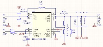
C14, C15, C16, C17 - ceramic capacitors; C21 - low ESR type

  • Welcome to the Forum.

    Short circuit tests are stress for the whole system including everything connected. With a short and releasing the short you can trigger oscillations which can cause overvoltage at supply or load connections. The PCB layout is important as well to make the circuit robust against a short.

    The schematic you have posted basically looks ok to me.

    40mA input current looks high to me even with PS/SYNC tied to GND. This already may be an indication that something is wrong with your circuit or test setup.

    Can you please share more information (either post it her or send it to me via private message if you do not want to publish it) about the layout and the test setup. It would also be helpful if you can share oscilloscope measurements of VIN, VOUT and inductor current.
  •  Thanks for reply.

    I tested the chip on two different PCBs. On each of PCBs the  TPS63070 behaved in the same way: it drew high input current without load (approx. 40 mA) and was damaged when the output was shorted to ground. First I noticed the problem on my first PCB and I decided to make another one (a small "evaluation board") to investigate the problem. The "evaluation board" contains the same components as the first one.

    The interesting thing is that even damaged chip responds to EN signal correctly - with EN pulled low, the input current is extremely low. I also noticed (with the use of ohmmeter) that damaged chips have L2 terminal shorted to ground.

    When it comes to setup, the board was powered from Hameg HM7042 power supply and HM8142 was used a active load (the HM8142 is two channel power supply 0..30V and each channel can also work as an active load).

    The inductor waveform is impossible to take for as I don't have a current probe.

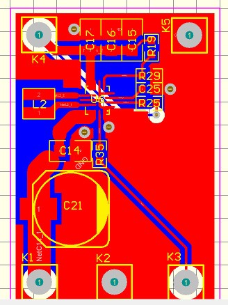
    I attached the PCB layout. Top layer is red and bottom layer is blue. The bottom layer contains only GND polygon and one track connected between "K3" terminal with EN signal of TPS63070.

  • I don't think that you get a reliable circuit with this layout. We have a recommendation in the datasheet (section 11.2). I suggest to copy that as close as possible.
    I think the GND connection of input and output is the weakest part here which most likely causes the failures during short circuit testing. The loops to the input capacitors and the output capacitors must be as narrow and as low impedance as possible. For this reason I would also recommend to add smaller capacitors closer to the IC in parallel to the existing capacitors (C1 and C4 in the datasheet recommendation).
    If you follow the datasheet recommendation you also will recognize an improvement in thermal performance. The IC will not get as hot as in your design and it will less likely shutdown because of overtemperature.

    For doing simple testing to get familiar with the device you don't need to design a PCB yourself. I recommend to use one of our EVM's for that.
  • I don't believe the layout is the problem. I had the chip assmbled also on different layout with 0603 capacitors directly at the TPS device terminals. The layout was almost the same like the one in the datasheet. Please take into account the fact that the converter works very well under normal conditions with 500 mA output current - no instability problems, ringing etc. If the layout was bad it would not work as expected. If the chip is so sensitive to the layout it makes it useless. I've been designing also SMPS power supplies for years and never had such problems with PCB layouts. Also, it seems to me that high quiescent current is not due to the bad layout but to something else. 

  • Regarding the no load input current you are measuring I recommend to read this application note. Since you are operating in boost mode (5V to 9V) measuring 40mA at the input in forced PWM mode seems possible to me.

    The observation of the high input current 450mA indicates to me that parts of the power switches are damaged and cannot be turned off anymore. This damage is caused by overvoltage, which means the breakdown voltage of the internal power FETs has been exceeded.

    If I compare our layout recommendation to the layout you have posted, especially the output loop (VOUT - COUT - PGND) I guess the parasitic inductance in the layout you have posted is at least 5 times higher than what we have in our recommendation. This directly translates in a voltage overshoot during switching which would be at least 5 times higher as well. The worst case occurs at the highest current. You have that when applying the short at the output. During the short it may be even more severe if the inductor saturates due to the higher current during the short.

    I think, if you are looking for a DCDC converter which works on a layout similar to what you have posted TPS63070 is not a good choice. In this case I would recommend to look for a device operating at a lower switching frequency. The lower switching frequency usually comes together with slower switching which means you get less problems with parasitics on the PCB. If you want a small solution for your given operating conditions, the higher switching frequency of TPS63070 of course is a key advantage. But unfortunately higher frequencies are related to tighter requirements on PCB design and component selection.

    If you follow the datasheet recommendations for the application design you will get a reliable converter as many of our customers did already.

  • The layout recommendation is not simply a thing that can be copied to every application. There are some constraints that must be followed when designing PCB (limited space, placement of the components, etc.) As I have told it before, I also used TPS63070 on different PCB layout - much better that one I posted in this thread and it also failed to work. The datasheet does not tell anything about parasistic impedance value (or maybe I overlooked something), but it states the TPS63070 has built-in overvoltage protection. It is extremely difficult to predict and to design PCB layout to achieve particular parasitic impedance value. If the TPS63070 is really so sensitive to the PCB layout it is very risky to use the device. The parasitic parameters can change with temperature - even in the best layout. This could also make the TPS63070 to work incorrectly. I can agree that the damage may be caused by overvoltage but I really can't imagine how this can be induced be parasiting iductance which is extremely low.

  • The built in overvoltage protection is described in the datasheet section 8.4.8. It prevents the device from damaging itself when either the output voltage feedback does not work properly or too much power is fed back to the input. It cannot protect the device against too high voltages which are connected to the pins. The voltages the device can handle are specified in the datasheet section 7.1 and 7.3.
    For further debug of your circuit I recommend to measure those voltages with appropriate measurement equipment. Can you please post measured waveforms of voltages at the pins VIN, VOUT, L1 and L2.
  • I packed the waveforms in zip file.2364.waveforms.zip

  • I examined different chip - MAX17112 (boost converter). I works very well without problems. Short circuit does no harm to the chip. Also, the input current at no load at the output is below 1 mA (with TPS63070 is 40 mA  !). Althought MAX17112 requires more external components, it suits me fine. It is evident that there is something wrong with the TPS63070.

  • Unfortunately there is no information about the settings of the oscilloscope you have used. The curves indicate that the bandwidth you are using for the measurements is far too low. You need to use a setup which has an appropriate resolution for capturing rise and fall times of 2ns, at least when you measure the voltage at the switch nodes L1 and L2.
  • If you only want to convert 5V to 9V TPS63070 is not a good choice anyway since it is a buck boost converter supporting functionality you don't need.

    What you need for converting 5V to 9V is a boost converter like the Maxim device you have selected or TPS61087 as an example for a converter from TI. You may find other options if you use our WEBENCH search tool, entering your requirements.

    For layout implementations like the ones you prefer I already recommended devices with lower switching frequency. Higher voltage rating of the power stage will also give you more margin for dealing with the higher voltage overshoots which you get with the higher parasitic inductances in the output loop.

    The difference of the input current at no load is related to the different power architecture of the different devices. This is not an indication that TPS63070 has a problem.

    Since I understand that you found a solution for your problem, I will close this discussion now.