This thread has been locked.

If you have a related question, please click the "Ask a related question" button in the top right corner. The newly created question will be automatically linked to this question.

TPS62740: Switching node waveform

Part Number: TPS62740

Hello,

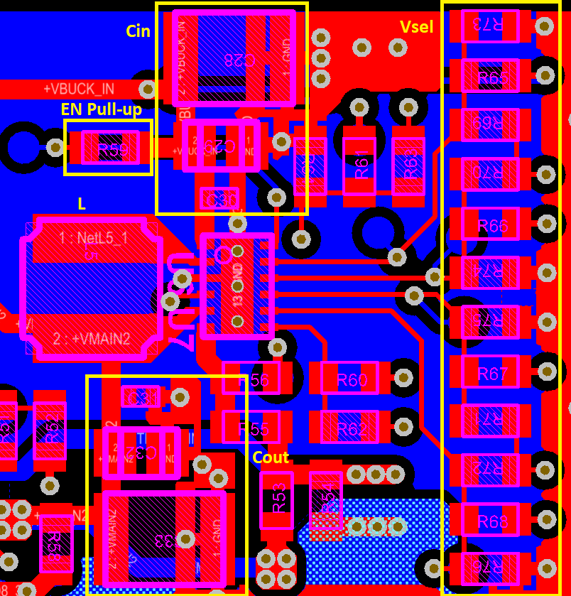
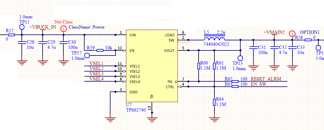
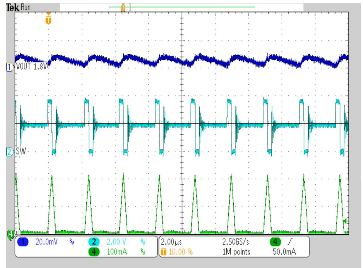
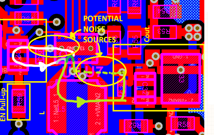
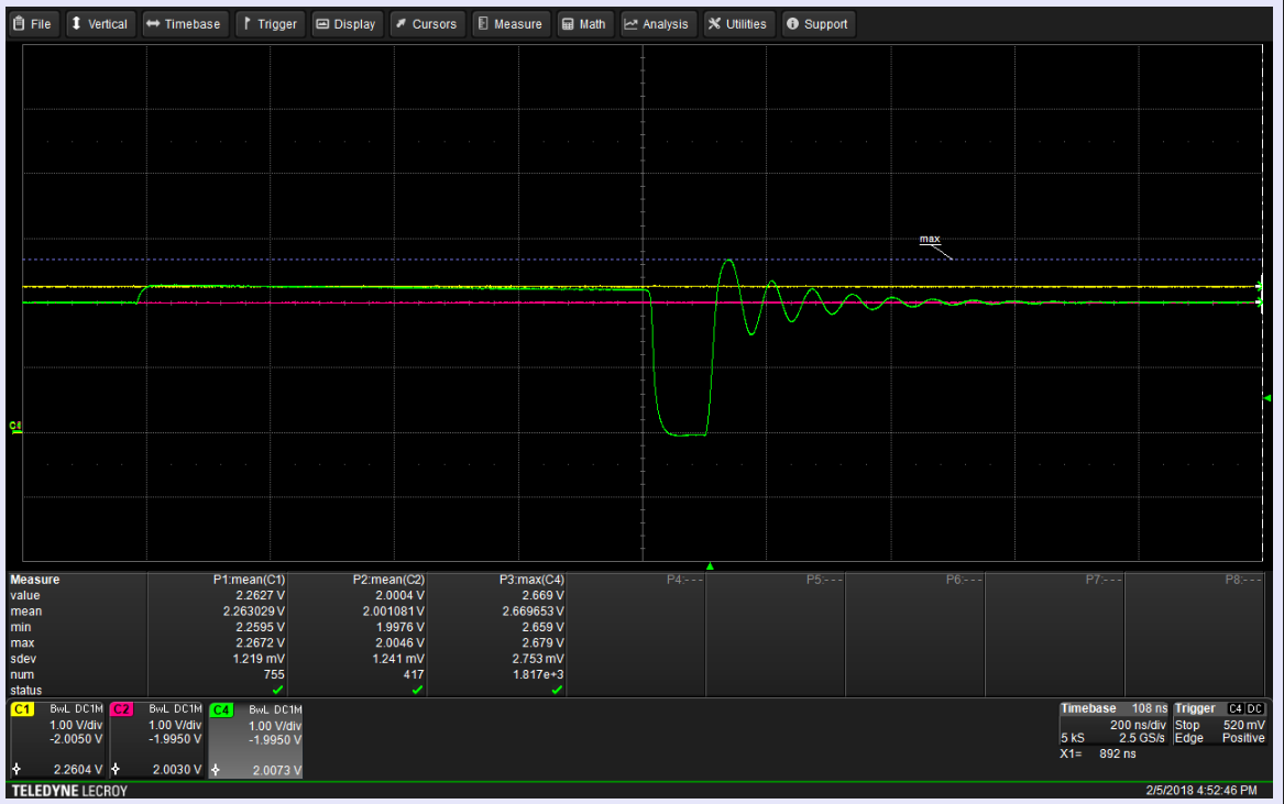
I'm measuring the voltage on SW node of the TPS62740 and I see these behaviour:

The absolute maximum ratings are:

-0.3V (in this case in more!!!) and Vin+0.3V (in this case more: Vin+880mV)

This behaviour is related to a not good compensation, usually. But i cannot act on the feedback loop (inside the chip).

Can you help me in this analysis, please?

Thank you and kind regards

Alessandro

  • Hello Alessandro,

    the behaviour you see is not related to the compensation. This is caused by the interaction of the switching pin with stray inductances/capacitances.
    Hence, I am talking about the layout, but most importantly the way you are measuring the SW voltage. The scope's probe must have the ground loop as short as possible, in order to minimize the inductance associated to the loop, hence shifting to higher frequencies the resonance freq of the measure circuit.

    I would suggest you to have a look at this video, which shows the techique I am talking about (even if referred to output ripple, the concept remains the same):
    training.ti.com/measuring-vout-ripple-dcdc-converters

    If your measurement is already correct, then you should have a look at your layout. If you want to share it with us, we could give you some advice.
  •   Hello Emmanuel,

    I did the measurement exactly in the same way of the video, BUT i didn't use the 20MHz bandwidth limiter.

    With this setting on the oscilloscope, we removed the negative glitch that you see on the scope in the previous message, but we still have the dumped ringing on the upper part, that is above the maximum ratings.

    Attached you can find the PCB (top layer=red) of this part of the circuit.

    Mid layer 1 is a complete GND plane, Mid layer 2 is Power plane, and Bottom layer (blue) is again GND+some tracks.

    Attached you can find also the schematic.

    I will wait for your comments/suggestions.

    Thank you and kind regards

    Alessandro

  • Hello Alessandro,

    the confirmation of a correct measurement is a great step forward.

    Regarding the damped oscillations, there is nothing to worry about. Below is reported an extract from the datasheet:

    Since this device is featured with Power Safe Mode, it uses Pulse Frequency Modulation. Hence the inductor is meant to completely discharge in the output cap,  and then the SW node is put in high impedance state until the inductor gets recharged.

    This means the converter is operating in Discontinuous Conduction Mode. The ringing of the SW node waveform is due to the resonating tank given by the inductor and the output capacitor in series with the parasitic capacitance between the SW node and ground. Since the output cap is orders of magnitutd bigger than the parasitic ones, it can be simplified as a voltage generator for the duration of the switching cycle. As a consequence, the DC value of the SW node will be Vout.

    In the datasheet's waveform, this damped oscillation can be noticed, which confirms that yours is a normal operation of the device.

    Having a look at your schematic and layout, I have noticed that the LOAD pin should be open, while in the layout is connected to R55 and R56 (not present in the schematic), Though, the CTRL pin seems to be connected on both board and schematics. I would do a sanity check of this feature from yours side, even if still I don't see which influence could have on the overvoltage on the switching node.

  • Hi Emmanuel,
    that's clear for me that this node have to be ringing, and I agree that is due to DCM, so the L will discharge on the output cap.
    What I'm trying to underlying is that the ringing (that in the picture from datasheet is below Vin+0.3V) in my case is above Vin+0.3V (ABS max rating of the component!)
    I would like to understand why this happen in my case, and how I can mitigate it/solve.
    For the load pin, I deleted the external connection on schematic, but we have a load connected to that point, don't worry.
    Waiting for your feedback, I wish you a nice day.

    Alessandro
  • Hello Alessandro,

    it's nice to hear that the LOAD function on your circuit is wanted and is under control.

    In the meantime I was having a look at your schematics and in parallel did some measurements on the TPS62740EVM.

    I can notice your layout is not following the rocommendation from the datasheet below. You can notice how the ground path of both Cin and Cout is very tight, and making the GND pin of the device the only one affected by the switching currents

    While on the layout you showed, the connections are very loose (below), increasing the parasites effects.Plus, the Cout is connected to the GND pin through vias and ground plane, which worses the radiated emissions effects. 

    On my measurement setup, I have tried to reproduce your operating conditions on the EVM:

    Vin=2.3V

    Vout=2V

    Iout=10mA

    Obtaining the following waveform:

    My recommendation is to follow our layout guidelines on the datasheet, and in general to make sure that pulsing currents have short paths and do not pass through vias.

  • Hi Emmanuel,
    I agree with your considerations on the PCB side. I will try to improve it in the next revision, as you suggest.
    Anyway there is one thing that is not clear for me: I see that also in your screenshot form your oscilloscope, you have the max voltage in the SW pin that is Vin+0.4V (Vin=2.26V; Vsw_max=2.66V; above the max rating of the component).
    How can it be possible?
    Thank you and kind regards

    Alessandro
  • Hello Alessandro,

    the abs max specification on the SW node is there to prevent the body diode of the HS switch to conduct continuously, putting the device in danger. In the EVM case, that value is overcame by 0.1V for less than 10 ns, which is too less to let the diode start the conduction.
  • Ok Emmanuel,
    Thanks for your explanation
    Have a nice day

    Alessandro