This thread has been locked.

If you have a related question, please click the "Ask a related question" button in the top right corner. The newly created question will be automatically linked to this question.

UCC28C42: Feedback Part of Flyback Circuit

Part Number: UCC28C42
Other Parts Discussed in Thread: TL431

Hi,

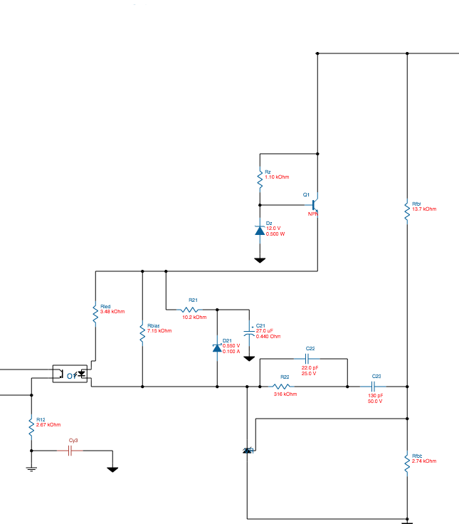
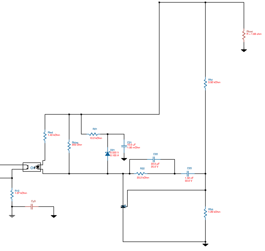
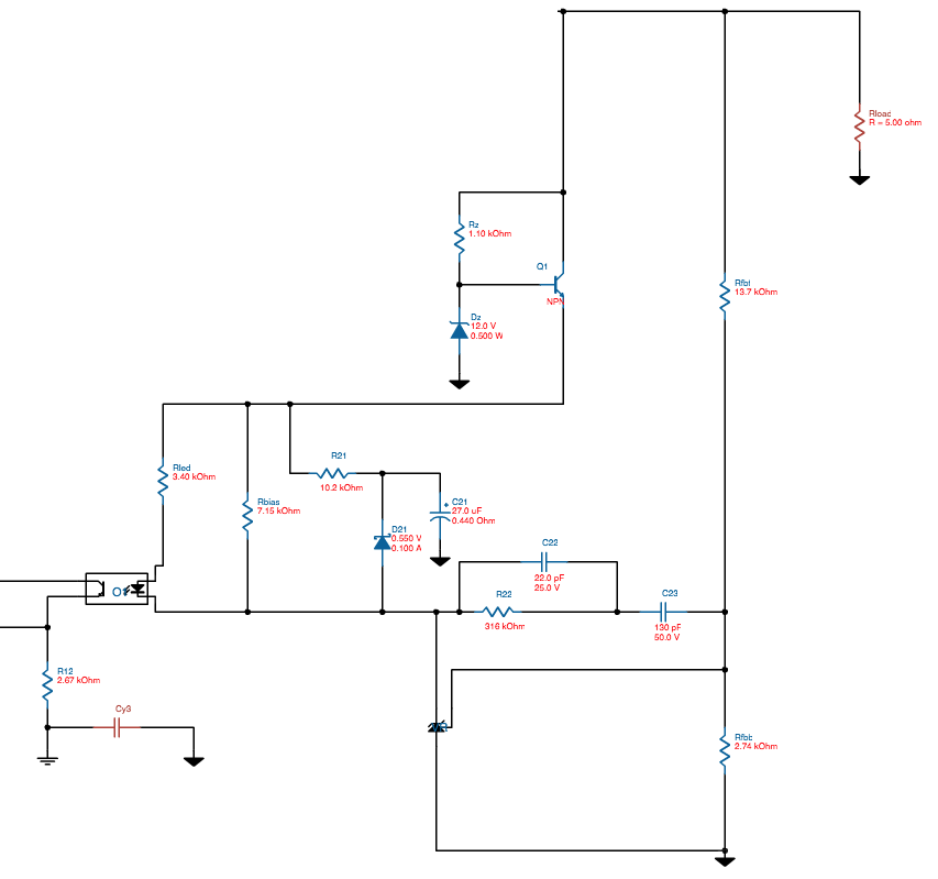
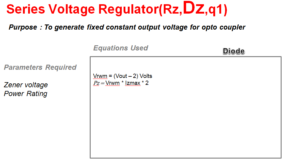
Could anyone please give me a detail explanation of the feedback part of this circuit attached (the second image)?

This circuit is from WEBench using the following specifications: 100-240V input, output 15V@3A using UCC28C42 controller.

  • Azhar,
    Thanks for the interest in TI here. I've contacted an applications engineer to support you. You should hear from them soon.
    Regards,
    John
  • Hello Azhar,

    Thank you for your question, below is a applications report on compensation design with TL431 this will be a great reference for you. Section 2.3 talks about the compensation network for flyback topologies.

    Hopefully, this will answer your question.

    Please hit Answered if you think this was helpful.

    Thank you,

    Sonal.

  • Hi Sonal,

    Thanks for the response.

    Could you please explain difference between Figure 4 in the PDF you linked and the screenshot in my original post?

    What the difference between having Rbias in parallel to the optocoupler in Figure 4 of the PDF and having Rbias in parallel to Rled+Optocoupler in the screenshot?

    And what purpose do R21, C21, and D21 serve in the screenshot?

    Thanks

  • Hello Azhar,

    There are two major differences between the two networks:

    1. The webench model has R21, C21, and D21 as extra elements; now to be very honest you do not need these. I would recommend leaving them NC. 
    2. The compensation network is a little different, C23 is in series with C22||R22, which is a different type of compensation.

    The TL431 acts as a transconductance amplifier and is recommended to have a bias current of 1mA, Rbias provides this bias current. There is no difference between the two connections as long as the current requirement is met.

    I hope this answers your question.

    Thanks,

    Sonal

  • Hi Sonal,

    Could you please describe the difference between the two compensations? Is there a design documentation where they go through the calculations for the values? The UCC28C42 datasheet doesn't seem to have the C23 series capacitance in the typical application section.

    Could you also let me know how important the Rz Dz and Cz components are in the TL431 application note you linked to? Because in the WEbench model seems to have Rz and Dz but with a BJT.

    Additionally the WEbench for a 5V@3A design does not seem to have Rz Dz while the 15V@3A design does. Below I have screenshots for both

    Could you explain what the significance of Rz Dz and Q1 are in the 15V@3A vs none of those in the 5V@3A?

    Thanks

  • Hello Azhar,

    As mentioned in the Application note Rz, Cz and Dz are there to basically clamp the voltage feeding into the anode of the optocoupler. when there is 5Vout there is no need for this clamping unit. 

    Also to answer your previous question: R21, D21  and C21 are there for ensuring the soft start operation, the Zener discharges the cap when the system shuts down. If this diode is removed then there will be effectively 2.5V/15Vout and 1.25/5Vout on Pin3 at startup from the voltage loop, and this will jeopardize the Soft start implementation and might lead to a system overshoot.

    I will forward the query about the difference between the compensations to the appropriate team for the correct set of equations.

    Thank you,

    Sonal

  • Hi Sonal,

    Thanks for the reply.

    I was going through the TL431 application note you posted before to design the feedback circuit.

    The application note seems to have a Rpullup resistor that doesn’t shows up on the WEBench schematic. But the emitter of the optocoupler seems to be connected to a resistor to ground, R12.
  • Hello Azhar,

    Please find the design calculations below, 

    The application note is an ideal way of designing the feedback, in practical applications pull up resistors are not required because the current from Pin8 is internally limited. As far as R12 is concerned it is just an RC filter for the FB pin.

    I hope this has answered your questions.

    Please hit Answered if your query is solved.

    Thank you 

    Sonal