Hi
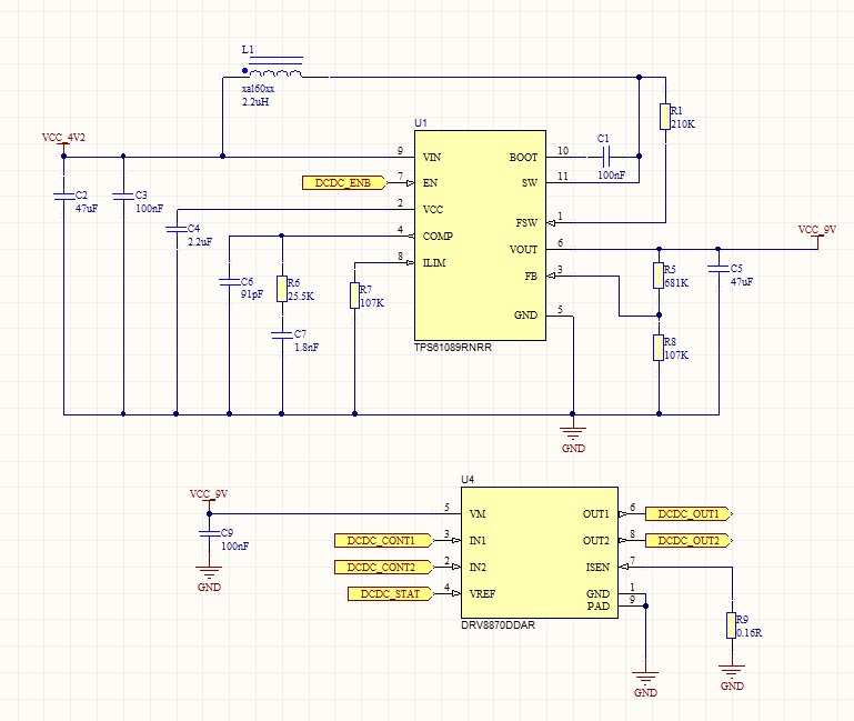
I am using the TPS61089RNRR to generate 9V 1.5A from a 4.2V 2000mAH Li-poly battery. Once the 9V is generated i am powering the DRV8870DDAR, to control the required solenoids.
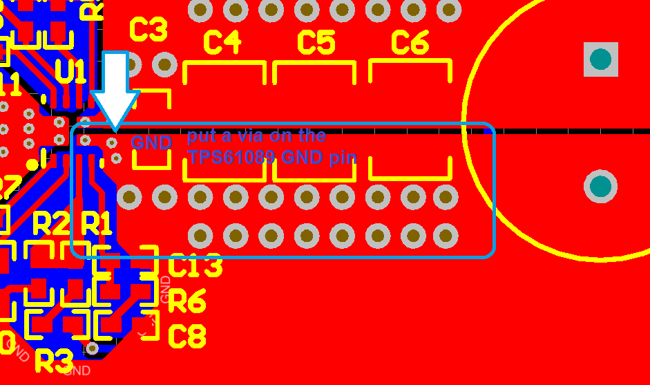
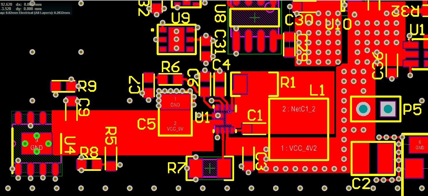
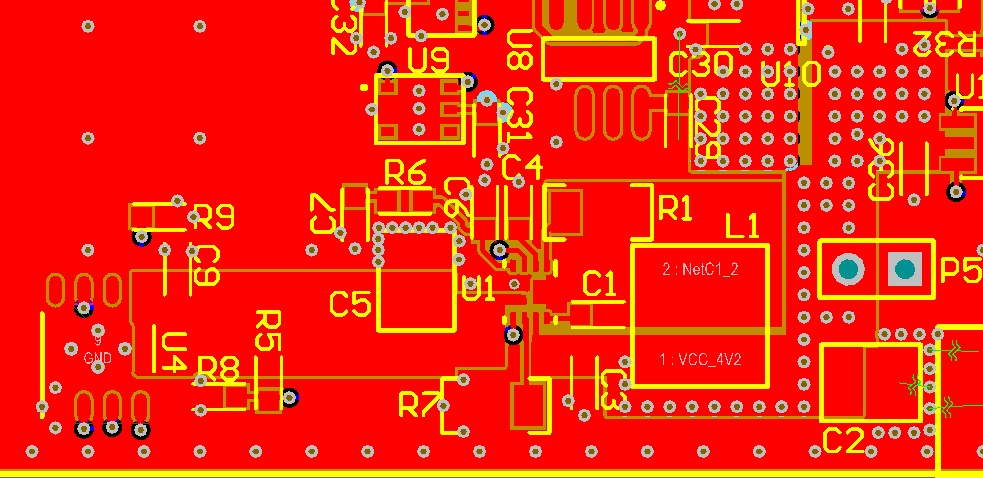
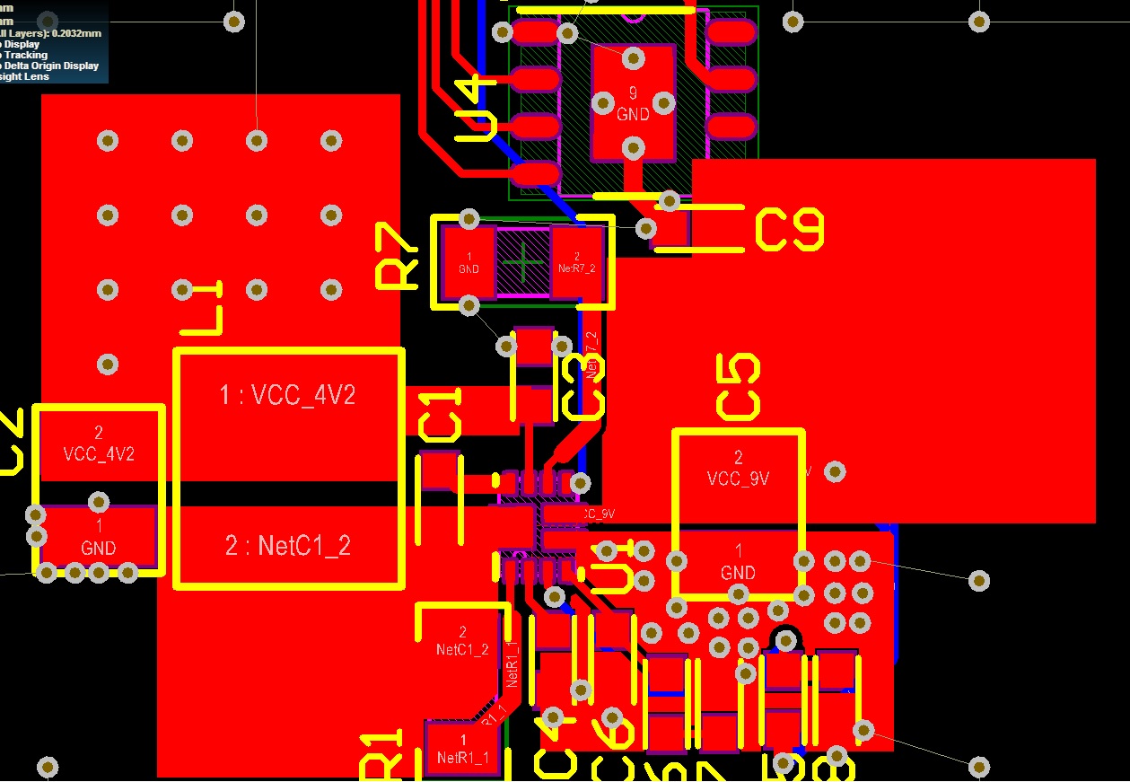
Please find my schematic and PCB layout below.
 .
.
I would like to know:
1. VCC_4V2 is 4.2V. It is directly connected from the battery to the VCC layer. From the VCC layer, to comes to the TOP layer copper pour using the 17 vias shown. Would this be an efficient way of doing this or should there be more vias?
2. The 9V is outputted onto a copper pour on the top layer, which is then used by the DRV8870DDAR?
3. The copper pour are all on the TOP layer only, should a identical copper pour also be placed on the bottom layer, with multiple vias?
I would appreciate if someone could kindly have a look into this Layout for any possible issues?
Thanks