This thread has been locked.

If you have a related question, please click the "Ask a related question" button in the top right corner. The newly created question will be automatically linked to this question.

Understanding inner current control loop compensation in boost PFC converter.

Other Parts Discussed in Thread: UCD3138A, UC2854B, UCD3138

Hello TI,

I am a NEW hire in our company and I am trying to understand the Analog PFC in our current design using L4981A PFC controller IC.


I need to fully understand the feedback control portion in this circuit because we are having some input current oscillation problems (Dancing waveform that is non-sinusoidal).

I am referring to the L4981A's application note for help. You can access it in this link: 

http://www.st.com/content/ccc/resource/technical/document/application_note/94/6e/ec/8c/4c/3e/40/a9/CD00003936.pdf/files/CD00003936.pdf/jcr:content/translations/en.CD00003936.pdf


We have plans to move into TI products especially the UCD3138A IC family of digital PFC solutions.


My questions below are related to how to select compensation network values for the inner current loop of Boost PFC.


Doubts from pages 7,8 & 9


The equation below is trying to say that the inductor down slope must be smaller than the ramp up slope of the PWM ramp that sets the switching frequency.

Inductor ramp down slope (we are seeing form negative side of sense resistor, before GND) is during Boost MOSFET turn ON so the voltage across inductor should be Vin and NOT VO like it is shown in the equation below right?


What is the value of the current amplifier gain? Is it made up of low frequency gain and high frequency gain referring to figure 9.

Actually the multiplication,  ( VO/L . Rs . Gca ) is the quantity of gradient that is output from C/A  right?


From page 9,

How is the voltage Vrs equal to below? I do not understand how Vrs is found by taking the input voltage (gradient), Vrs of +ve terminal of C/A and multiplying it to 1/S ?

What is the meaning of worst condition here? where did this integrator with DC pole come from?


What is the quantity Gavg ?


How did Gavg come to be as shown below? What is its physical meaning?

Why is Gavg multiplied to Gca? Are they combining two transfer functions? Is Gca the high frequency transfer function or Gavg? What is the reason to split them?

The crossover frequency comes to the above after I equated Gca . Gavg = 0'


Where did the zero come from in the below equation? Gca is not frequency dependent and Gavg only has an integrator with DC pole so where did the zero come from?

Also why is there a zero in Gca around 6000 Hz in the below graph? Where did it come from?

Please also give the closed loop final transfer function of the compensation network shown in Figure 9


Please help to answer my questions as I try to understand the current loop compensation portion of this PFC boost converter. We are moving into TI products although we find them to be quite advanced.


Thank you for your help.


Regards,

Peeterson.


PFC BOOST LOOP-COMPENSATION COMPENSATION FREQUENCY-RESPONSE CURRENT-LOOP COMPENSATION- NETWORK


  • Hello Jose
    The L4981A is an ST part and you should contact ST for any support you need.
    TI make the UC2854B which is a superior part and there is a comprehensive list of support document that will answer any questions you have.
    The document folder is located here:
    www.ti.com/.../technicaldocuments

    Regards
    John
  • Hi John,
    Thanks for your reply.

    The concept of CCM Average current mode control is same in both the ICs. Could you please help to answer my questions if you know their answers?

    We are going to develop a 2.5KW PFC for wirebonding machines in Singapore. It will use TI digital PFC.

    If I can understand the current design it will be helpful in the new design.

    Quite frankly, ST customer support is rubbish! so I resorted to TI's help!

    Please answer me if you know.

    Thank you and sorry for the inconvenience.


    regards,
    Peeterson
  • Let this post be here. I will find the solution myself and reply for the benefit of others...
  • Hi Peeterson,

    Since you will find the answer by yourself, I will close this question. By the way, thanks for planing to use UCD3138A for your PFC solution. Please go to TI website and search UCD3138, there are lots of supporting documents for UCD3138 controlled digital PFC solution.

    Regards,
    Bosheng
  • Hi TI,

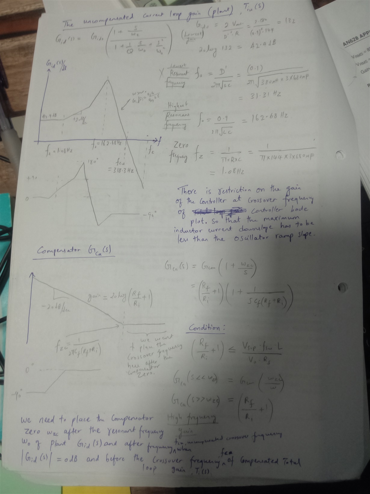
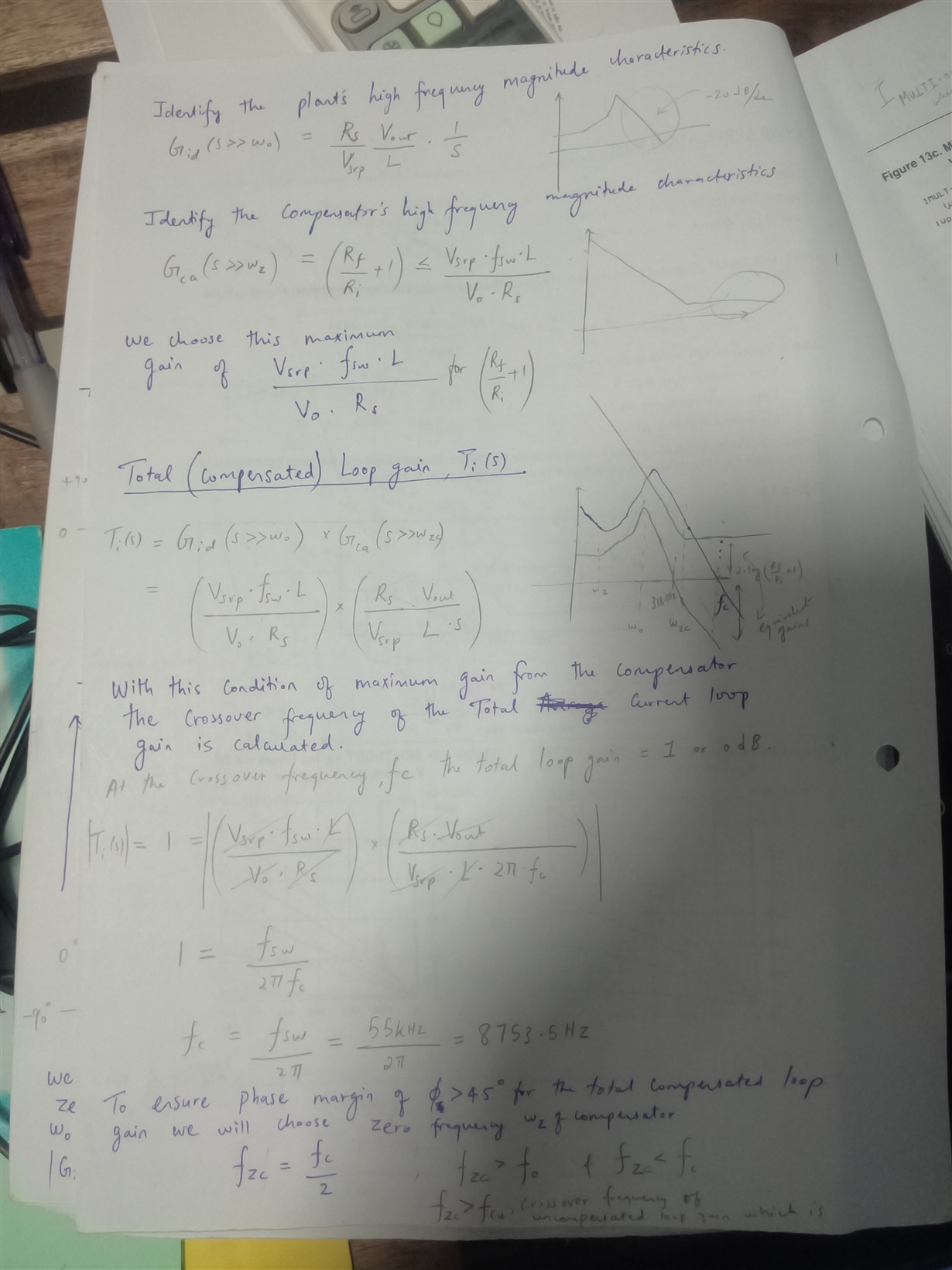
                I had promised to investigate this issue for the benefit of others so I have. I will elaborate on the summary below in the next post.

    Inner current loop transfer function without compensation and with compensation can be found from the video lectures in coursera in the link below.

    https://www.coursera.org/learn/current-control

    Go to week 4 ->  Average Current Mode Control -> Video: 4.7 Introduction to PFC rectifiers and design example

    you can understand the transfer functions there.

    Basically, you need to shape the (Compensated current loop) bode plot so that you get (1/2)*fsw bandwidth, sufficient phase margin, high DC/Low frequency gain.

    You have to do this with the help of constraints like PWM ramp slope should be greater than inductor current downslope because negative current is sensed so it is NOT the inductor current UPSLOPE.

    I will update on this soon with photos of my handwritten notes.

    Thank you for your patience.

    regards,

    Peeterson.

  • Hi Peeterson,

    Thanks for sharing this. Looking forward to your notes.

    Regards,

    Bosheng

  • The transfer functions are simplified around the frequency of interest by cancelling high frequency or low frequency poles/zeros. These notes plus the video on coursera and the application note are sufficient to understand the operation and modification of the inner current loop in PFC;

    Thanks,

    -Peeterson.