This thread has been locked.

If you have a related question, please click the "Ask a related question" button in the top right corner. The newly created question will be automatically linked to this question.

BQ24618: no charge with VCC lower 5V

Part Number: BQ24618
Other Parts Discussed in Thread: BQ24617

Good morning,

I've red another thread with the same subject, but it has been close, so it is not possible to reply:

e2e.ti.com/.../559386

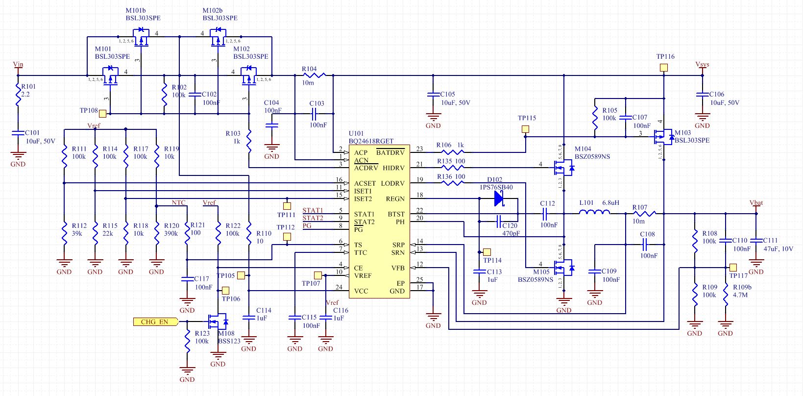
I've got the same problem: the body diode of the input MOS reduces the Vcc at startup below 4.7V. It could be the reason why my charger dosn't start with a standard 5V input 8e.g. from USB).

Is there any way to fix this issue?

Thank you and regards

Matteo

  • Hello Matteo,

    Can you please show your schematic? and your measurement? 

    Have you tried using the same FET that is used on our EVM?

  • Hello Jing,

    here is the schematic:

    When Vin=5V, the Vcc is a little below 4.7V (Vcc=4.6V). When Vin=5.1V, Vcc=4.7V and charger starts to charge the battery.

    The problem is that, accordingly to USB specifications, Vin can also be as low as 4.75V. In my design I've chosen the BQ24618 because it is declared to work with a minimum Vin of 4.7V and to be "USB-friendly".

    There are no EVB for BQ24618. If you are asking about the BQ24617 EVB (but BQ24617 has a minimum Vcc of 5V, so it has a specific difference on parameter we are discussing about), no, I'm not using the SI4401DY pMOS, but the BSL303SPE.

    Thank you and regards

    Matteo

  • sorry, maybe the schematic picture is missing in my previous post:

    Matteo

  • I've selected the pMOS BSL303SPE instead of SI4401DY because of its ID vs VGS characteristic.
    The BSL303 is suitable to be used with a single cell battery because it assures a good on state also with a VGS lower than 3V. Such characteristic is necessary for the M103 pMOS (see my schematic), but I decided to use only one pMOS model in my design (because no special requirements for M101 and M102 pMOSes were no specified in BQ24618 datasheet).

    Matteo

  • What is the battery voltage you are testing with? Also how are you connecting the battery?

    To begin charging, VCC must be higher than SRN by at least 500 mV (otherwise, the device will be in sleep mode). TI recommends an input voltage of at least 1.5 V to 2 V higher than the battery voltage, taking into consideration the DC losses in the high-side FET (Rdson), inductor (DCR), and input sense resistor (between ACP and ACN), the body diode drop of RBFET between VCC and input power supply, and battery sense resistor (between SRP and SRN).

    Therefore, there are a lot of add on resistance that our charger cannot control. Selecting FET with lower Rdson, lower DCR inductor, and shorten the trace between input to IC, and IC to the output will help to reduce the resistance on the high current path.

  • Hi Jing,
    I have already checked and the Vcc voltage is properly higher than SRN (more than 500mV).
    Battery is a li-ion single cell (voltage range: 3 to 4.25V) and Vcc comes fron a USB port (voltage range: 4.75 to 5.25V).
    Accordingly to what you say, there aren't 1.5 to 2V of difference, but such a recommendation is not so evident in official TI document, where, instead, it is clearely pointed out that the BQ24618 is "USB friendly", i.e. is compatible exactely with standard voltage ranges I have in my application.
    Anyway I repeated my tests also with a low battery (3.8V) and the problem is the same.

    Each parassitic resistance shouldn't enter in any evaluation about the problem I have because the charging phase in my case doesn't start and so no curernt is flowing through such elements (i.e. no voltage drops appears along tracks and components).

    What about to add a schottky diode in parallel with MOS M101, in order to reduce the voltage drop on its internal diode?
    Does it make sense? I could try if it works...

    Thank you and regards

    Matteo
  • Sorry Jing,

    in my previous post I made a mistake: Vin is more than 600mV higher than SRN, but Vcc not (because of the body diode of M101).

    So maybe you are right: when the battery is high, the BQ24618 does not exit the SLEEP mode:

    • battery full charge voltage (i.e. SRN voltage): about 4.2V
    • Vin minimum voltage: 4.75V (USB)
    • Vcc minimum voltage: 4.3V (depends on MOS body diode)
    • SLEEP rising voltage (Vcc-SRN): 0.1V, well below 600mV (i.e the SLEEP rising threshold)

    How can the BQ24618 be "USB friendly"?

    I've checked my proposed solution of a schottky diode in parallel to the M101 body diode and the situation is much better. The problem is not completely fixed, but it is restricted to only worst cases.

    What do you think about such workaround?

    Is there anothe solution? Is it possible to disable the SLEEP mode?

    Thank you very much

    Regards

    Matteo

  • For 5V USB application, you can remove the reverse blocking FET. Instead you can add a zener diode at the input for reverse plug protection.