Hello,
I am working on a boost converter using LM5022 on the bench. No input power. Feedback loop is connected by Vout remains at 0V.
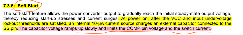
Objective: I would like to control SS pin externally so that to control the duty cycle. The info is very limited in the datasheet. Need your help.
What I did is: use a voltage divider with Vcc pin (Vcc=7.5V measured by DMM) to control SS pin voltage. Vin = 12V is given by bias voltage power supply.
When Vin=12V, Vcc = 7.5V, SS pin is found by DMM about 3.1V (by changing the trimmer pot in the voltage divider with Vcc). However, OUT pin of IC remains low. No gate signal even at start up.
At start up, I can only see SS ramp up by about 3.1V. No gate signal.
Since there is no real input voltage into boost,1) I notice that CS pin remains low. I didn't add any external resistor at CS pin to create slope compensation (not yet). According to TI-TINA, I would add 1kohm for stability.
My questions:
1. Can I control SS pin externally so that to control the duty cycle? (actually to control peak-current command)
2. If we cannot, is there any way we can do this? How about control COMP pin directly so that peak-current command under control. It may be susceptible to noise. Is this recommended to do so?
3. How does SS pin control the internal EA? Please give more info.
4. If no real input voltage into boost and switch current remains zero, and COMP pin voltage remains pretty high, like 3.7V. In this case, will output duty cycle becomes maximum, given CS remains around 0V?
5. Can SS pin overwrite EA no matter what? Or SS pin only works for certain time window during start up?
Thank you in advance
YZ
.