This thread has been locked.

If you have a related question, please click the "Ask a related question" button in the top right corner. The newly created question will be automatically linked to this question.

BQ24725A: Cannot charge over 12ish volts. Anything over 12V shuts off the Input FETs

Part Number: BQ24725A

Hello,

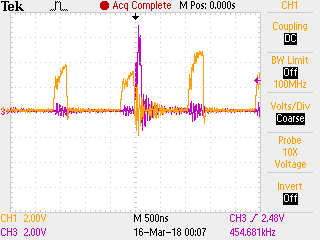
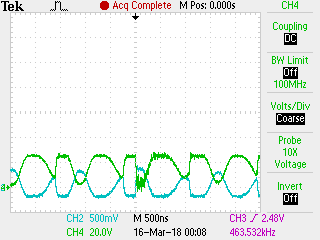
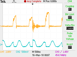
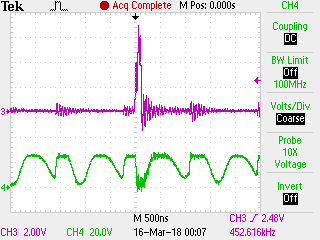
I have a working circuit I used last year that TI recently made a few tweaks to and now the charge voltage won't go above 12ish volts without shutting off the input FETs.  Changes I have made from the last working design to now include the following:

- Changed 5m sense resistors to 10m sense (for max current of 8A, 5m was able to get me to do up to 16A)

- Changed the inductor from 3.3uH to 4.7uH  (wouldn't see this being an issue, 4.7uH is used on the TI demo board of the design).

Any help on where to look would be appreciated

Thanks, Mike

  • Change 5mohm sense resistor to 10mohm and change inductor current from 3.3uH to 4.7uH should not affect the output voltage loop regulation.

    "the charge voltage won't go above 12ish volts without shutting off the input FETs."
    Would you give more detail about "shutting off the input FETs"? Do you mean the output voltage going up after shutting off the input FETs?
  • Thanks for the information.  I've been using the BQ evaluation software to set the option, charge current, charge voltage, and input current registers.  When I'm setting the voltage register, I can go as high as about 12V (verified with a meter connected where the battery would go).  If I try to set it to 13V then the meter goes off and I check the input FETs and they're OFF (the ACFETs).  If I try to set the voltage back down to 12V or below, nothing happens and I have to power cycle the PCBA and start over.  

    Hope this helps

  • Now, let debug which protection or loop control limits the output to 12V.
    1. What is the input voltage? What is the battery voltage? Does the sleep comparator (VCC to SRN comparator) turn off the ACFET?
    2. When ACFET is off, what is the ACOK voltage and ACDET voltage?
    3. Could you disable IFAULT_HI and set IFAULT_LOW to "1"?
    4. What is the ACFET's extra Cgs and Cgd value? Can you share the charger portion schematic?
  • I will gather the requested information.  Here is requested schematic:

  • For item 4, you can try to reduce C6 from 0.1uF to 0.047uF and Cgd from 2200pF to 1000pF.
  • My apologies for the delays, weather in the northeast kept me out of the lab for a couple of days last week.  Responses to your questions:

    1. What is the input voltage? What is the battery voltage? Does the sleep comparator (VCC to SRN comparator) turn off the ACFET? 

    Input voltage is 24V, battery voltage is what we are trying to set.

    Measured VCC to SRN measurements with a scope, when I set the output voltage to 12.288V was about 11.2V.  When I tried to set the output voltage to 13.312V this jumped up to ~22.5V but dropped to 10.2V prior to this happening.  This should not be in sleep mode then correct?

    2. When ACFET is off, what is the ACOK voltage and ACDET voltage?

    ACOK = 3.3V (pulled up w/ 10K)

    ACDET = 2.77V


    3. Could you disable IFAULT_HI and set IFAULT_LOW to "1"?

    This seemed to work.  However I didn't need to do this on the previous setup that I mentioned (with different inductor & sense resistor).  Where would you suggest that I start troubleshooting for why I'm tripping IFAULT?


    4. What is the ACFET's extra Cgs and Cgd value? Can you share the charger portion schematic?

    Changed these to match what you stated previously (Ggs to .047uF, Cgd to 1000pF).  No change in the performance.

    Thanks, Mike

  • Thank for the testing result. From the item 3, we know the root cause is from the IFAULT. Now, we can continue working on the root cause of IFAULT:
    a. disable IFAULT_HI and set IFAULT_LOW to "1": which one work?
    b. check the HIFET; LOFET gate drive waveform and switching node waveform to make sure:

    1. No shoot through between HIFET and LOFET

    2.HIFET or LOFET is turned on in 100ns when HIDRV or LODRV signal starts turning on.

  • Thank you, please see comments in red.

    Wang5577 said:

    Thank for the testing result. From the item 3, we know the root cause is from the IFAULT. Now, we can continue working on the root cause of IFAULT:
    a. disable IFAULT_HI and set IFAULT_LOW to "1": which one work?  IFAULT_HI appears to be the culprit
    b. check the HIFET; LOFET gate drive waveform and switching node waveform to make sure:  

    Here are settings used w/ BQ Bench Test Software:

    - Option register set to 0x9832 (IFAULT_HI is disabled, LO is 135mV

    - Charge Current = 4096mA

    - Input Current = 8064mA

    - Charge Voltage = 16800mV

    **NO battery actually installed so no charge current is flowing.

    Colors on all scope shots:

    - Yellow is TOPFET, Vgs

    - Blue is TOPFET, Vds

    - Purple is BOTFET, Vgs

    - Green is BOTFET, Vds

    1. No shoot through between HIFET and LOFET

    Taken at no charge - timing of TOP Vgs vs BOT Vgs


    Taken at no charge - timing of TOP Vds vs BOT Vds (this should show any shoot through


    2.HIFET or LOFET is turned on in 100ns when HIDRV or LODRV signal starts turning on.

    Below are images of Drive (Orange/Purple) vs the FETs ON/OFF (Green/Blue)


  • Thank you, please see comments in red.

    a. disable IFAULT_HI and set IFAULT_LOW to "1": which one work?  IFAULT_HI appears to be the culprit

    b. check the HIFET; LOFET gate drive waveform and switching node waveform to make sure:  

    Here are settings used w/ BQ Bench Test Software:

    - Option register set to 0x9832 (IFAULT_HI is disabled, LO is 135mV

    - Charge Current = 4096mA

    - Input Current = 8064mA

    - Charge Voltage = 16800mV

    **NO battery actually installed so no charge current is flowing.

    Colors on all scope shots:

    - Yellow is TOPFET, Vgs

    - Blue is TOPFET, Vds

    - Purple is BOTFET, Vgs

    - Green is BOTFET, Vds

    1. No shoot through between HIFET and LOFET

    Taken at no charge - timing of TOP Vgs vs BOT Vgs


    Taken at no charge - timing of TOP Vds vs BOT Vds (this should show any shoot through


    2.HIFET or LOFET is turned on in 100ns when HIDRV or LODRV signal starts turning on.

    Below are images of Drive (Orange/Purple) vs the FETs ON/OFF (Green/Blue)


  • 1. disable IFAULT_HI and set IFAULT_LOW to "1": which one work? IFAULT_HI appears to be the culprit
    2. From the test waveform, the HIDRV turn-on takes about several hundreds ns. It could be too long. So, the protection circuit measures a high voltage across the HIFET due to the slow turn-on.
    So reduce the BTST and HIDRV series resistor value or select low Qg FET can fix the problem.
  • Thank you. My BTST and HIDRV series resistors are currently 0 ohms so can't do much reduction there. Any recommended Qg values? I'm currently using Infineon BSC0901NSI, Qg is currently 4.1nC which seems very low. Turn on time should be 5nS for this FET.
  • If that is the case, the issue could come from the layout. The datasheet page 34, figure 21 and 22 talks about that.
    If we cannot change the layout, we have to disable the IFAULT_HI protection.
  • Hello

    I misspoke on a couple of the numbers previously stated.  I had said that the Qg is 4.1nC, that was for QG(th).  The total Qg for this component is around 20nC for a Vgs of 4V (measured in previous scope shot).  As you can see from the previous schematic sent over, I have two FETs in parallel on the top to help split the power loss across the two parts instead of one.  My assumption is that this would double the capacitance and charge on the gate, so I removed one of the FETs as a test.  I am no longer tripping the IFAULT_HI, and it looks like my rise time is about 100nS.  See scope shot below (yellow is now with 1 FET, grey is before with 2 FETs).

    Wang5577 said:
    If that is the case, the issue could come from the layout. The datasheet page 34, figure 21 and 22 talks about that.
    If we cannot change the layout, we have to disable the IFAULT_HI protection.
    Didn't look like it was this.  I am not using the "system current" anyway, only the charge current.  Below is a screen shot of the sense reading anyway, how does this look? Red is the top component layer, purple is one of the inner ground layers.  I highlighted the sense lines in white.

  • I think you find the root cause: the high Qg slows down the turn-on time and make IFAULT_HI. Please find some low Qg FETs to fix this problem.