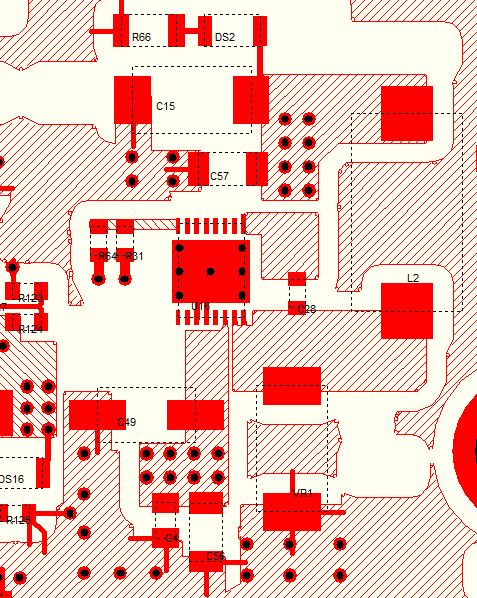
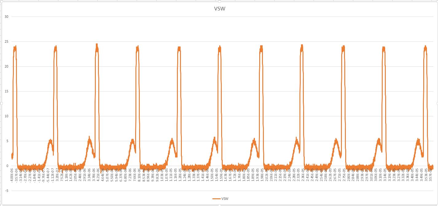
I have a new design using this part to convert 24VDC to 12VDC. I am getting 0VDC on the VSW pins with little to no steady-state current draw on the 24VDC that is connected to VIN.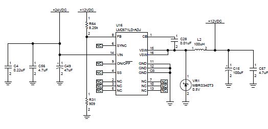

-
Ask a related question
What is a related question?A related question is a question created from another question. When the related question is created, it will be automatically linked to the original question.