This thread has been locked.

If you have a related question, please click the "Ask a related question" button in the top right corner. The newly created question will be automatically linked to this question.

TPS53319: TPS53319 high HF noise

Part Number: TPS53319

Hi,

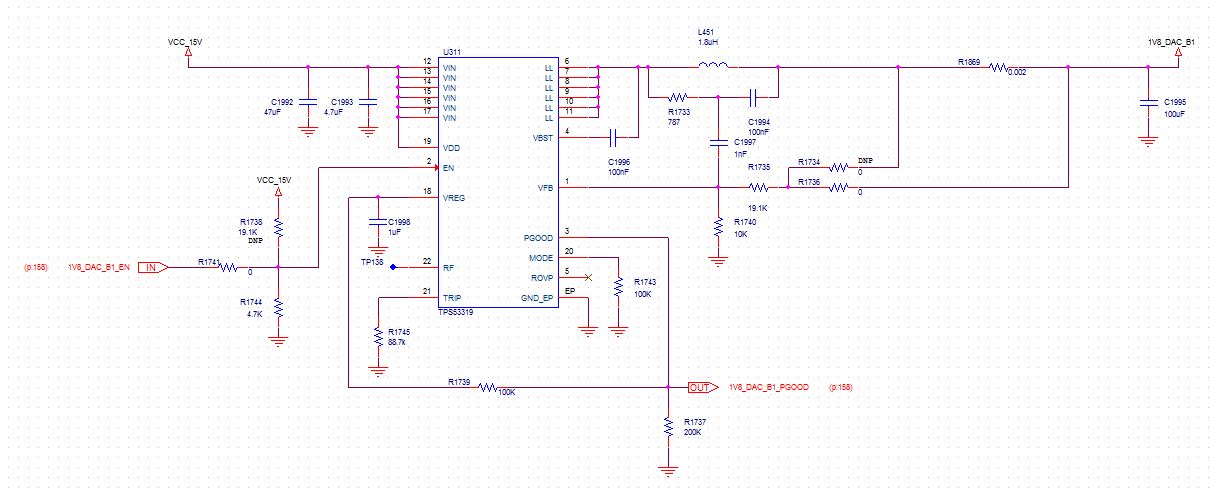
I had integrated on my design some TPS53319 configured based on WEBENCH designs.

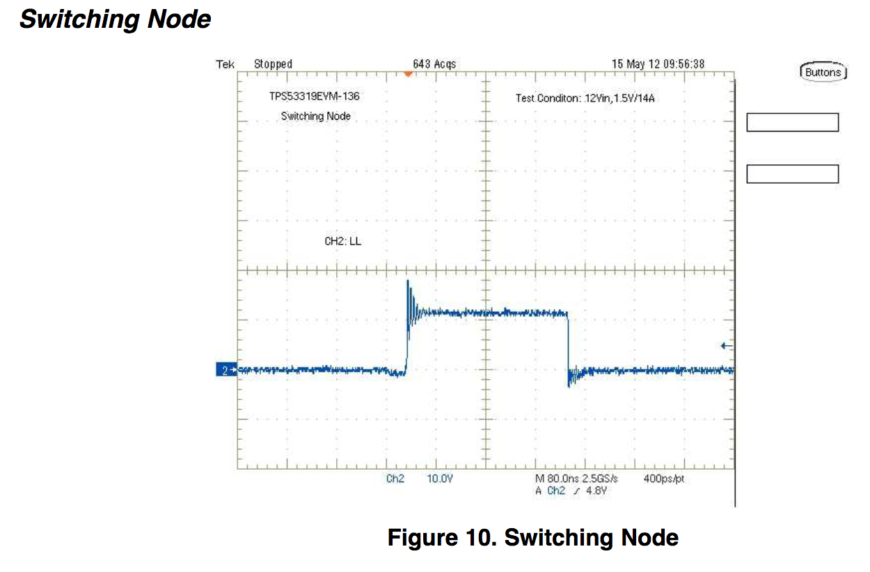
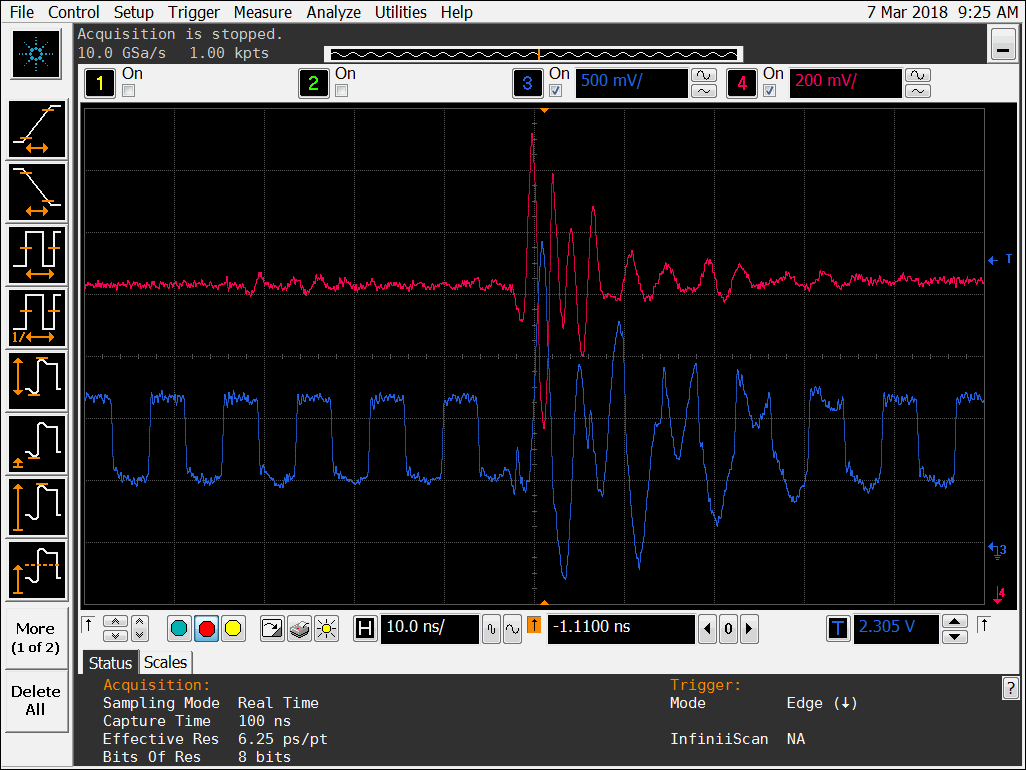
My system is actually characterized by an high HF noise due to ringing oscillations.

I had measured these HF spikes on both input and output nodes.

This noise actually afflicted some LVDS signals and makes my system fail.

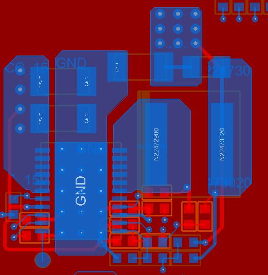
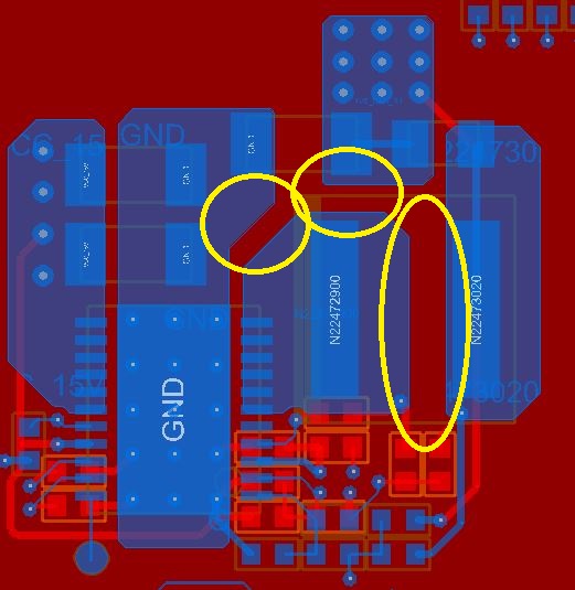
Here you can see that this noise afflicted the clock node.

This spike played as common mode noise but its amplitude bring each single ended signal out of their 1.8V rail.

Is there any way to reduce this spikes?

I tried with both snubber nets and resistor in series with Cboost but I had no practial results on that.

Thank you,

Ranieri A.

  • Alessandro,

    What are the waveforms you are showing?  Can you share your schematic and layout?

  • Hi John,

    Sure, I'll posted down here a snapshot of my schematic and Layout.

    What I showed it's just one of the DCDCs output embedded on the board (violet waveform) with its HF spike noise due to the ringing.

    The blue waveform is just  one of the signals corrupted by this coupled noise.

    I can capture same ring noise (higher in amplitude and not showed in scope screenshot) at the input node too (VCC_15V) and in this case this is the net who drives the digital net to move its common mode.

    Consider that I have different DACs with same digital interface on my design and just couple of them fail the interface test.

  • Any update about your schematic and PCB layout? Or did you resolve your issue already?
  • Hi John,

    I posted in previous post two pictures but then I discovered they're not showed in forum,

    I'll try again:

    Here my schematic on this DCDC

    Down here a snapshot of the Routing

  • I don't see any issue with the layout or schematic.  You will always get some switching noise on both input and output.  Here are some things you can try Two of witch you have already done:

    1.  Resistor is series with the BOOT capacitor.  I don't know what values you tried but typically 2 ohm to 10 ohm is effective.

    2.  RC snubber from SW to GND.  I will enclose a document to help you optimize it.

    3.  You can also add HF bypass capacitors to your input and output 0.1 uF, 0.01uF, 0.001 uF, etc in parallel.  Each of these will have impedance minimums at progressively higher frequencies.  It looks like your ringing is about 250 MHz. so I expect 1000 pF will be the most effective.

    4.  If all else fails you may need to consider more extensive filtering such as ferrite beads or additional LC stage.

    4810.RC Snubber.pdf

    Let me know if any of this helps.

  • Good to know that layout looks correct,
    This would be a good starting point for a design review.

    As you said I tried with 1. and 2.
    I tried adding some HW bypass capacitors too but as far as I get I didn't get any consistent improvement.

    Refagarding 4., ferrite and LC for these board cannot be added since I don't have some 0Ohm series or other to intercept the input net.
    I can try something with the output stage since we have a series resistor for current sensing, I can skip sensing and adding a filter.

    I read about this post:
    e2e.ti.com/.../design-a-second-stage-filter-for-sensitive-applications

    Do I have to consider the second stage part of the loop or is it possible to add it OUT of the feedback loop?

    Thank you for article you post, I'll read it.

    Alessandro Ranieri
  • John,

    regarding routing I have couple of doubts:

    I'm comparing tps53319 datasheet layout example with TPS53319EVM-136 evaluation module routing.

    I had noticed that feedback components in datasheet example are placed on TOP layer while in EVM all the path is on BOTTOM side of the board.

    My layout follow datasheet example, does it plays a role on ringing amplitude?

    Improve in air gap between switching node and output node, as well as ground node will introduce some benefits?

    refer to circle: 


    Best regards,

    Alessandro Ranieri

  • That post is mostly effective for filtering out additional switch frequency ripple. You would want to have that outside the FB loop. You likely cannot compensate for 2 double poles.
    In your case that may or may not be effective anyway as your frequency is of interest is around 250 MHz. At that frequency parasitic effects tend to dominate. Any large value ceramic capacitor will be inductive at those frequencies. That is why I recommended multiple low value incremnts in parallel (0.1uF, 0.01uF, 0.001uF, etc).
  • Did you ever resolve this? Do you need any further assistance? let me know.
  • Hi,

    Right now I didn't resolve this issue.

    Right now I have some of the point you propose that I cannot applied to this design:

    Second stage filters

    Series Ferrite Bead

    I don't have series path in both input and output that let me free to applied this solutions.

    For a redesign I would like to understand if these approaches can be useful, can you confirm that with the TPS53319 EVM I would be able to generate ringing in order to test couple of these solutions? This will be necessary to be confident that a redesign will be effective.

    On the other side, on my design I can just try with

    snubber

    RC boost

    bypass capacitor

    Next days I would try with them but right now I don't have a board that I can use to test.

    If none of this works, I would redesign the system with other DCDCs so an help on this would be appreciated.

    Anyway I will follow up with results and waiting for you for a feedback on EVM.

    Best Regards,

  •  Enclosed please find a waveform of the SW node with ringing:

  • Thank you John,

    I would buy in couple of days EVM trying to verify improvements.
    I would follow up with this and any update on our design.

    It will take some days for sure.

    Regards,
    Alessandro