This thread has been locked.

If you have a related question, please click the "Ask a related question" button in the top right corner. The newly created question will be automatically linked to this question.

UCC28C44: UCC28C44

Part Number: UCC28C44
Other Parts Discussed in Thread: LM8364, TL431

Hi,

We have designed power supply based on UCC28CC44.

The requirements are as below:

VinMin = 62.0V
VinMax = 140.0V
Vout = 12.0V
Iout = 0.25A

The circuit is working as intended expect  as below:

1. The circuit is not switching OFF at 60V and It gets OFF only at 10V

Can you please help us to solve this issue? I am attaching the web bench  file for your inputs.

Thanks in advance.

Regards,

Rajesh.design inputs_UCC28C44DR_62_140_12_250ma_reviewed_1701.pdf


  • Hi Rajesh,

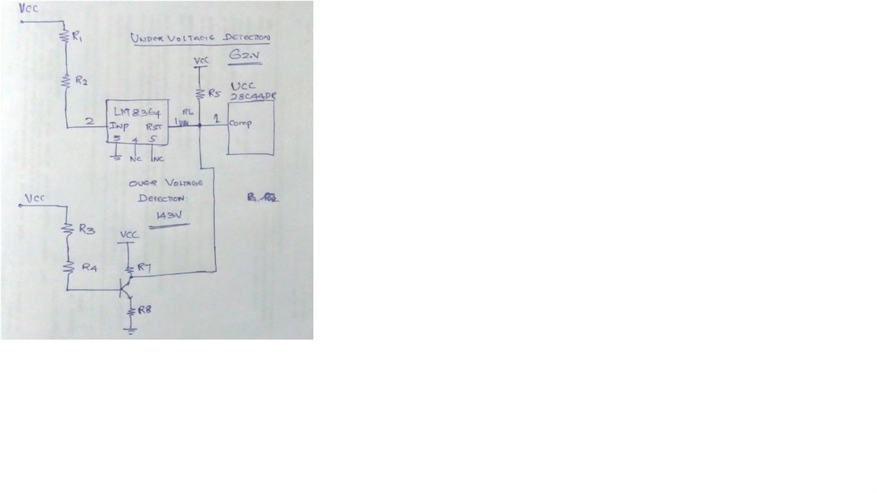
    Thanks for your interest in UCC28C44. This device will not turn off until VDD hits its UVLO threshold which is 9V typical. What you can do is use an external circuit connected to the COMP pin to pull COMP low when Vin is less than 62V to disable the converter. You could use an open drain comparator with an internal reference such as LM8364 and a resistor divider from Vin to disable the converter when Vin is less than 62V.

    Best Regards,
    Ben Lough
  • Hi Ben Lough,

    Thanks for your response.   This helps us lot.

    This system should operate from 62V to  143V AC.

    I have made quick hand sketch schematic for your inputs and advise attached.  I have included a small transistor logic to cut off at 143V AC.

    Kind request you to let me know your views.

    Thanks in advance.

     Regards,

    Rajesh

  • Hi Rajesh,

    You will want a resistor connected from INPUT to ground of LM8364 to form the divider. I would suggest not connecting a resistor from Vin to COMP, you will want the internal error amplifier to drive COMP under normal operation. You can connect a resistor from INPUT to RST to add some hysteresis to the UVLO threshold.

    For the overvoltage circuit, I would suggest adding a 75V zener and 68V zener in series with R3. This will give you a discrete threshold for when the overvoltage circuit engages. You will want a resistor connected from the base of the transistor to ground as well. I would suggest leaving R7 out of your circuit for the same reason as R5.

    Best Regards,

    Ben Lough

  • HI Ben Lough,

    Thanks for your valuable inputs.

    We have further continued our testing.  in any cases the voltage at COMP pin is not more than 6.31V and  OUT remains " 0V".

    The secondary output is 15.93V. 

    Can you please help me by providing your time to have web call any time today or tomorrow?  tomorrow would be the ideal time.

    Thanks in advance.

    Regards,

    Rajesh.

  • Hi Rajesh,

    Could you share your full schematic and any oscilloscope waveforms your have captured? Is VREF still 5V?

    Best Regards,
    Ben Lough

  • Hi Ben Lough,

    Thanks for your kind support.

    1. Yes VREF is still at 5.02V

    2. Kindly find the schematic scan copy attached for your inputs, Measurement points are highlighted and page 2 indicates the actual measurements.

    3. The requirements are as below:

    VinMin = 62.0V
    VinMax = 140.0V
    Vout = 12.0V
    Iout = 0.25A

    Please advise.

    Thanks in advance.

    Regards,

    Rajesh.Schematic_Scan.pdf6813.Schematic_Scan.pdf7701.PowerSupply.pdf6787.PowerSupply.pdf

  • Hi Rajesh,

    Thanks for the additional information. Could you check the FB pin voltage with Vin at 80V? Is it close to 0V? Also do you see switching operation at OUT with Vin at 80V?

    Best Regards,
    Ben Lough
  • Hi Ben Lough,

    Thanks for your time.

    1. The voltage at FB pin is 2.274 at Vin 80V AC.

    2. Yes.. The switching operation is happening at OUT pin. At 80V the OUT voltage remains " 0V"
    have reduced the voltage from 80 V to 0 at voltage 10 , the OUT is increasing upto to 4.5V and switches off, since the input voltage is 0V AC.

    Thanks in advance.

    Regards,
    Rajesh.
  • Hi Rajesh,

    What is the voltage of COMP? Because the FB pin voltage is less than the internal 2.5V reference, the controller may be pushing the duty cycle to its maximum. What is the duty cycle you see at the OUT pin?

    The TL431 is supposed to bias the opto so that the voltage on the FB pin increases when the output voltage is too high. What is the voltage across R12?

    Best Regards,

    Ben Lough

  • 3000.PowerSupply.pdfHi Ben Lough,

    Thanks for your kind support.

    1. The voltage at COMP is 6.24V and FB = 2.6V

    2. Voltage across R12 is " 0V"

    3.  I feel the problem lives here around  OPTO FOD 817. I'm measuring  8.6V at  pin 1 and 8.0V at Pin 2.  Very slow dis charge is happening on these pins, even  after  the main input supply is completely switched OFF.

    4. Pin no: 4 of Opto FOD 817 is always " 0V".

    Thanks in advance.

    Regards,

    Rajesh.

  • Hi Rajesh,

    I would suggest increasing your fast lane gain. Increase the resistance of R15 to ~10kΩ. Could also tell me the voltage across R14? I would like to know the forward current in the opto.

    The voltage on R12 should not be 0. It could be worthwhile to install a new opto-coupler to make sure this behavior is not due to damage to the opto.

    Best Regards,
    Ben Lough
  • Hi Ben Lough,

    Thank you very much for your kind support.

    1. Can you also please suggest me the capacitor value of C25? ( This is connected between 2 different grounds)
    2. Voltage across R14 is 8.67V.
    3. Voltage across R12 is increased to 1.66V after replacing with 10K. Sure will replace the opto coupler and come back to you.

    Thanks in advance.

    Regards,
    Rajesh.
  • Hi Ben Lough,

    Thanks for your kind support.

    1. We have replace the Opto - coupler and the observations are as below:

    2. The output pin remain at " 0V"

    3. U2 ( Opto) -   (Anode pin no 1) 8.63V,           (Cathode pin 2 ) 8.0V,           (Pin 3)  1.66V, (Pin  4) 5.02V

    4. Comp  =  4.17V,  FB = 2.5V,  CS = 0V,  RT - CT = 1.63V,  OUT = 0.48V,  VDD = 19.25V, VREF = 5.0V

    5. Increase in OUT up to 5V, if the input voltage decreases.  

    Thanks in advance for your support.

    Regards,

    - Rajesh.

  • Hi Rajesh,

    The capacitor you choose for the Y cap (C25) depends on your isolation requirement (3kV isolation needed, galvanic isolation, meeting any isolation standards, etc).

    Could you show me a waveform of the OUT pin at 140Vin?

    Best Regards,
    Ben Lough
  • Hi Rajesh,

    Are you able to share a waveform of the OUT pin at 140Vin?

    Best Regards,
    Ben Lough
  • Hi Ben Lough,

    Apologies for the delay in response.

    Unfortunately... the board is not working due to short.. will come back on this in couple days.

    Regards,
    Rajesh.