This thread has been locked.

If you have a related question, please click the "Ask a related question" button in the top right corner. The newly created question will be automatically linked to this question.

UCC28951-Q1: Duty cycle changing directly from Dmax to Tmin burst mode

Part Number: UCC28951-Q1
Other Parts Discussed in Thread: UCC28951

I tested my circuit with power section. My input voltage is 120V and o/p is 24V in CV mode. I am using external error amplifier. R7 is open and Output voltage feedback is only used. Vdac is set point and Vo_adc is o/p voltage f/b. Ideally when these two values match, EA+ should go low and UCC should control it as CV mode.

Ea+= Vdac-Vo_adc ...(unity gain).

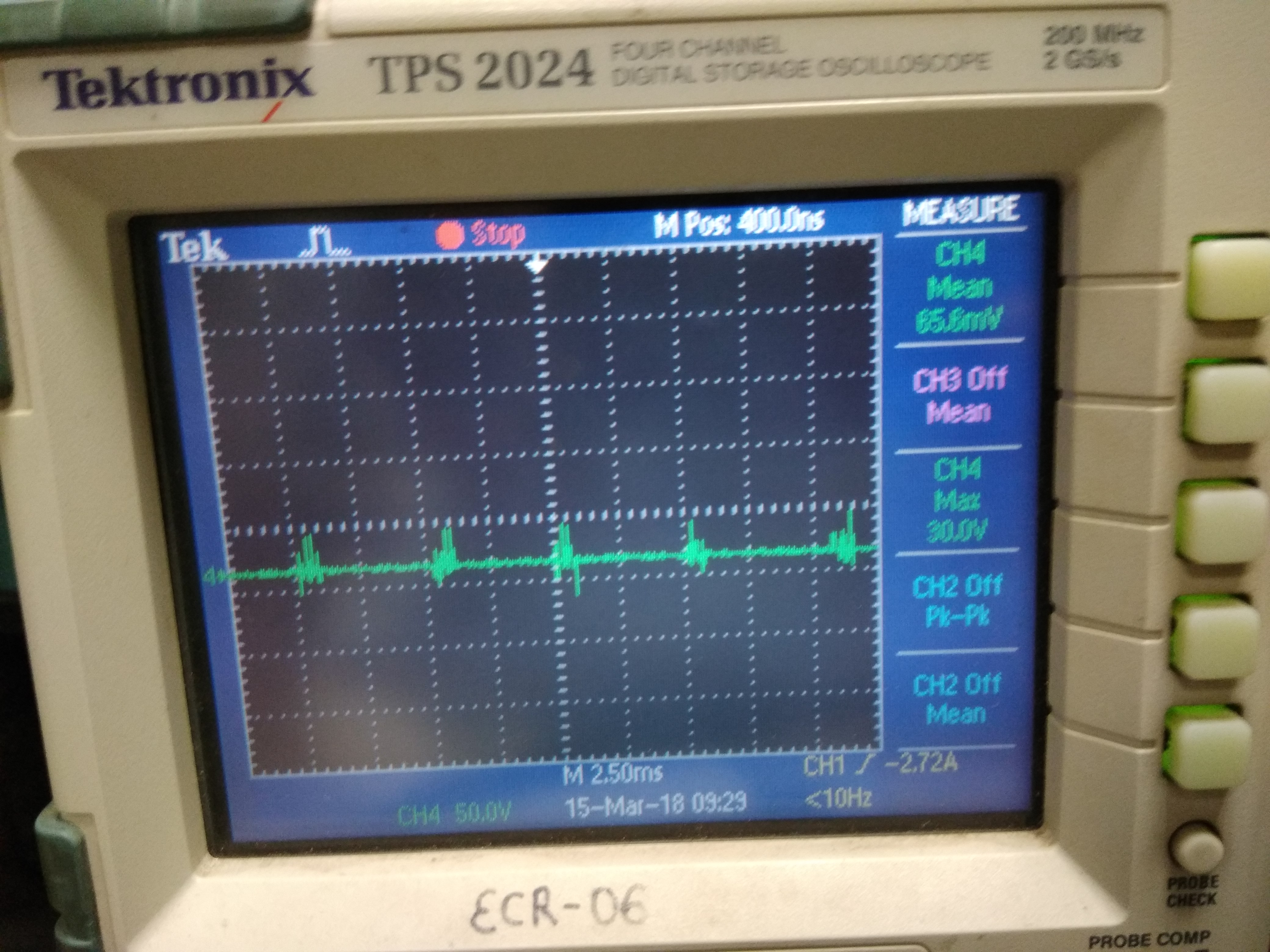
When I give Vdac =1.5 V and when Vo_adc = 0.7V, the system becomes unstable and magnetics start making noise and the unit enters in Desat protection. This happens aroung 0.8V @ comp pin. 

1. Should the opamp U45 be unity gain? (All its resistors are 10k making it unity gain differential amplifier).

2. Will the compensation loop values effect the basics controlling of the system? I tried changing it and calculating it based on the datasheet but there is no effect.

3. What will be Rsum effect?

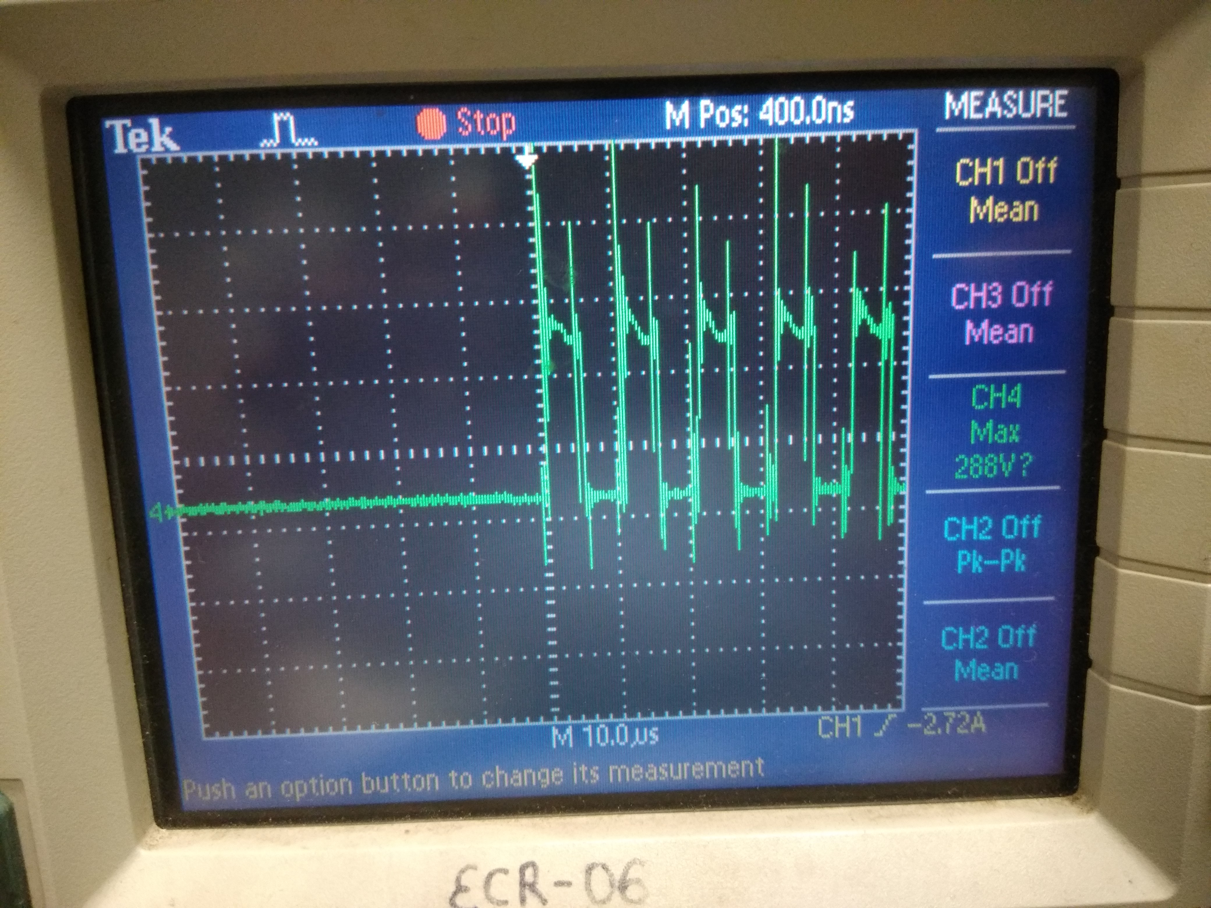
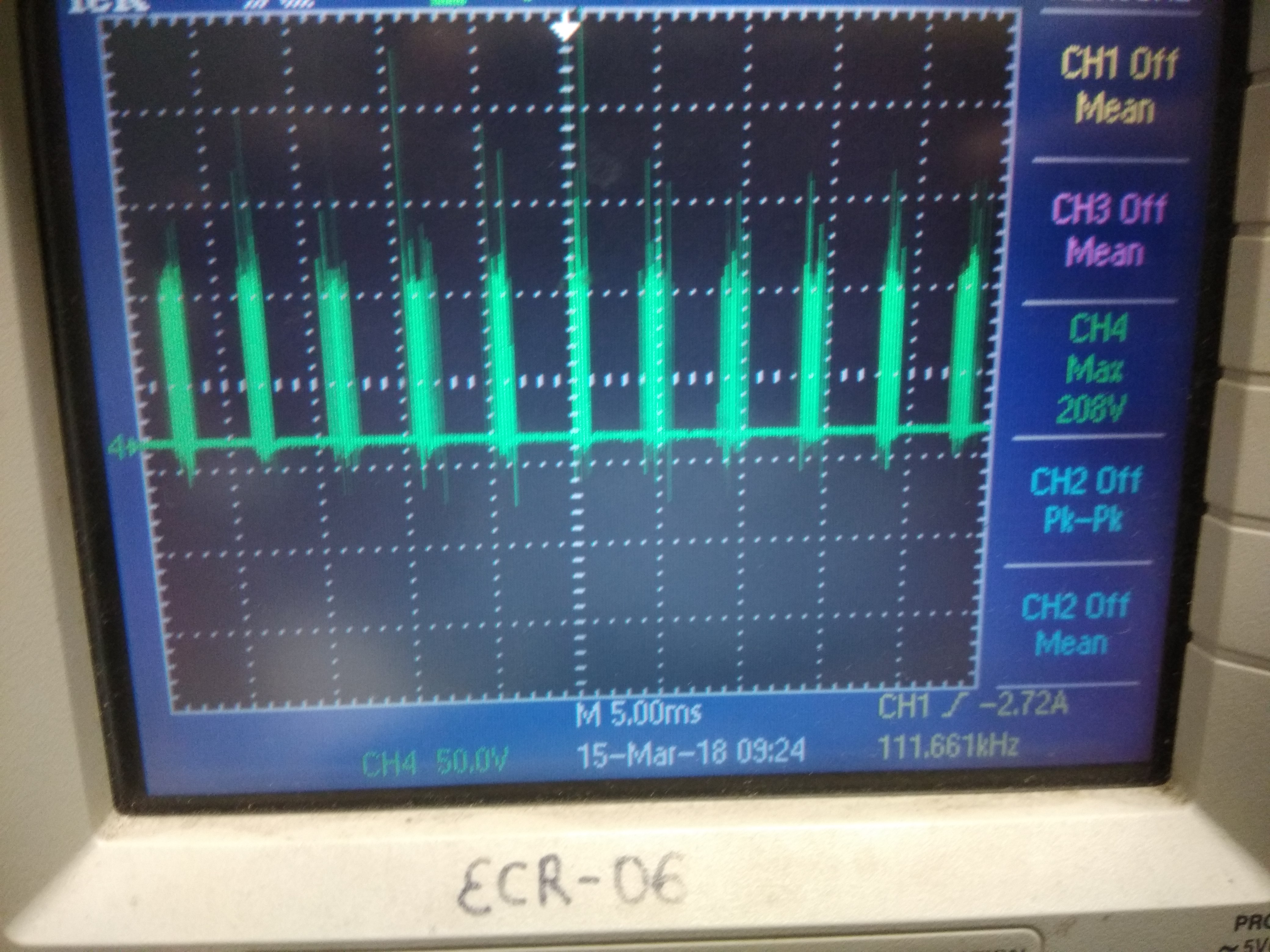
4. When I remove the voltage feedback the system gives 30V uncontrolled o/p at 95V i/p. Transformer is 4:1. But when I connect the f/b, the system starts misbehaving as mentioned above i.e. at 35V i/p and 9-10V o/p the magnetics start making noise and then there is desat. The Gate, Drain waveforms are very noisy and unclear.

Also, after making R123, R53 = 0ohms, and when set value for output voltage is kept at 16V then the controller keeps duty cycle at max till 64V (4:1 transformer) and after that if i increase the input voltage the duty cycle should vary but instead it directly goes into burst mode with changing the phase shift between switching MOSFETs. The magnetics starts getting noisy thereafter.

Can you suggest why the duty cycle is directly going from Dmax to Tmin burst mode?

Please suggest what should be the circuit values for making this work. Please let me know the effect of Rsum and Comp pin voltage.

Thanks,

Jignesh C. Patel

  • Hi Jignesh,

    We will need a day or two to look at this problem. We will respond soon.

    Regards

    Peter
  • Hi Peter,

    Earlier Rsum resistor was 10k from Rsum to Vref now it is 100k. I was able to get phase shift during simulation.

    Since, internal EA is uesd as unity gain buffer, I applied voltage at EA+ pin and same should be seen a COMP. I checked with diff values of voltage at EA+:

    1. 0.7V>EA+: Pulses Off

    2. 0.7V<EA+<1.2V: BURST MODE

    3. 1.2V< EA+ <2.9V : PHASE SHIFTED PULSES

    4. 2.9< EA+ : Dmax

    When I connected the power section, I was able to get CV at no load but that was with burst mode. So does UCC28951 always work in burst mode to achieve regulation?

    Because it tries to keep voltage at COMP pin around 0.7-0.8V so it will have to work in burst mode.

    Also, after loading it with just 0.25A load (200A is rated load), regulation was getting poor.

    Regards,

    Jignesh C. Patel

  • Hello Jignesh

    I posted a reply to your first query at e2e.ti.com/.../668195

    Let's use this thread for further posts on this topic - so

    Ucc28951 always works in burst mode at light loads. This happens if the required duty cycle falls below the threshold set by the TMIN pin. It is not possible to defeat burst mode. Note - operation at light load in burst mode is more efficient than operation continuously and the MOSFETs will run significantly cooler in burst mode.

    Please post the waveforms I requested in my reply to the first post and we can take it from there.

    Regards
    Colin
  •     Hi Colin,

    The waveforms are very noisy and are not clear.

    When I apply 0-120V input for desired output of 20V, the 20V o/p appears at 50V i/p and then it phase shifts till 65V and then goes in burst mode till 120V.

    My concern is why it stays in phase shifted mode for such small band i.e. 50-65V i/p only. Ideally at 50 V i/p and Dmax if 20V is output then even at 120V i/p we should get 20V in phase shifted mode with 20-30% duty cycle.

    Waveforms of drain source and CS pin attached. CS pin there is no signal, even if I disconnect CS pin from the circuit the waveform is same.

    Regards,

    Jignesh C. Patel

  • Hello Jignesh

    You are correct - the waveforms are very noisy indeed and to be honest I think that you will need to 'fix' these waveforms before you can expect the controller to give good results.

    The first place I would start is the PCB layout - The path from the input capacitor to the MOSFETs in the bridge circuit must be a low impedance - short, direct tracks - you probably have the current transformer in this path somewhere - that's ok. The connections from Drains of the lower MOSFETs to the Sources of the upper MOSFETs must be short. The connection between the Drains of the upper MOSFETs must be short. The connection between the Sources of the lower MOSFETS must be short.

    The length of the connection from the mid point of the Left Hand MOSFETs to the mid point of the Right Hand MOSFETs should  is not as important as that of the other connections I mentioned above. This is because any inductance in this path will add to the transformer leakage inductance.

    I don't like the way that the drain voltage seems to drop gradually when the MOSFET is off so I would also confirm that the high side gate drives are working properly.

    The layout of the output rectifier circuit should also be reviewed.

    I wold also suggest that you review the layout around the UCC28951 controller - make sure that NONE of the OUTx tracks run under the IC or parallel to any sensitive input - especially the CS input.

    You could run the system at a low input voltage - say 20V or so - it will run at Dmax but it will give you an opportunity to investigate your layout.

    The current sense signal is not a control variable in Voltage Mode Control  so you can safely tie that pin to GND for initial investigations. Just be very careful not to short or overload the output terminals, because without the CS signal you have no current limit protection - this is ok for initial investigations BUT not for the finished product.

    I would also consider removing the feedback circuit completely and controlling the duty cycle directly from a potentiometer at the EA+ input - as I described earlier. This will reduce the number of variables in the system and help to diagnose where the instabilities are coming from.

    Once you get the waveforms cleaned up you should notice an improvement in the systems behaviour (it may not behave ideally but it should work a little better)

    One small point is that you did not label the traces you posted - It makes it a little more difficult to understand what they are showing - it was ok in this case but in general a label helps.

    Let me know how you get on

    Regards

    Colin

  • Hi Jingnesh,

    It has been over two weeks since the last communication. If you have new information please start a new thread.

    Regards

    Peter