Other Parts Discussed in Thread: TPS61175
Hi,
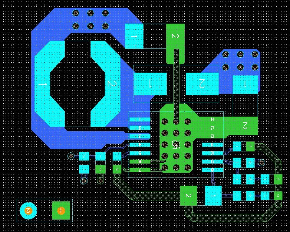
We are laying out a board now using the TPS61175QPWPRQ1. We have followed the layout notes per the datasheet and have come up with the attached layout. We are wondering about the following in the attached layout:
1) The path for Cin is quite narrow due to limits on the schottky diode pad location. Should this be changed to allow for a wider path? Or can/should components be moved around?
2) Is the Cin further away from the Vin pin OK?
3) This is a 14 layer board are we correct to just do the major routing for these components on the top layer were the parts are attached?
4) Are there any other updates or recommendations for layout for this part?
Thanks,
David'