


Hello,
I tried solving an issue with an UCC28711 for three days without success now and decided to post the question here. I read all articles I found in this forum and pdfs from TI related to the UCC2871X family, related parts and the TIDU873A "Leakage Current Measurement Reference Design for Determining Insulation Resistance", but it didn't solve my problem.
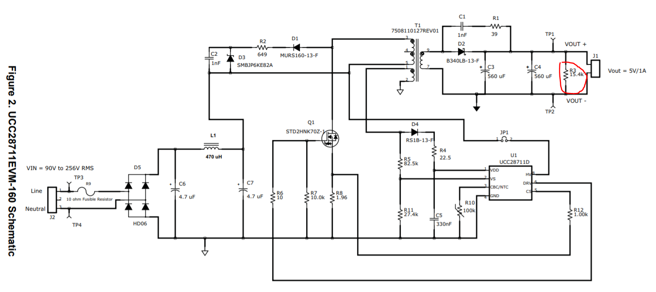
I designed an own PCB based on the TIDU873A, see schematics below. However, the UCC28711 won't start up properly - instead, it is only giving one pulse at the DRV pin and then presumably goes into fault mode. Unlike the datasheet proposes (8.4.4 Start-Up Operation) and the Reference Design as well (6.7.2.6 Power-On and HV Start-Up), my chip does not give three startup pulses and then decides to go into failure mode.

Oscilloscope Screenshots:
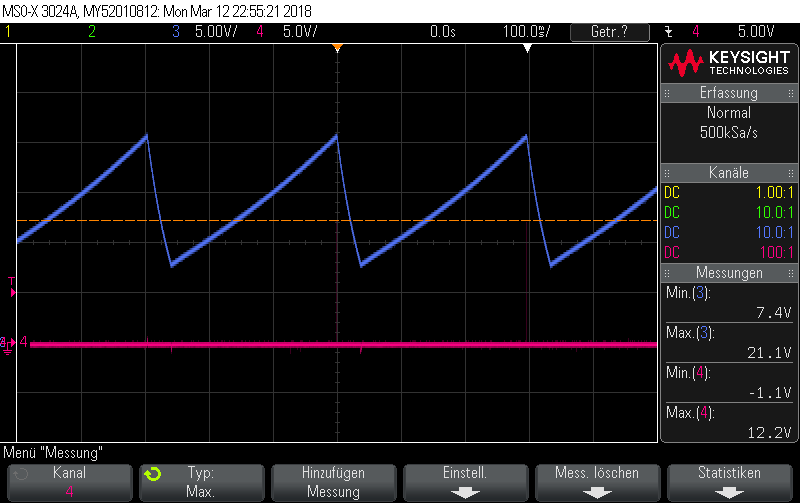
A.) VDD pin to GND_ISO (blue) and DRV pin to GND_ISO (red), with 100 ms/div and after that: zoomed in/retriggered with 1us/div
B.) VDD pin to GND_ISO (blue) and VP500_ISOWAE (output pin) to GND_ISOWAE (red), the two initially isolated Grounds being connected through the oscilloscope - no 500 Volts here, but 22.0 to 28.8 V.

C.) VDD pin to GND_ISO (blue) and VFB (auxiliary winding) to GND_ISO (red)

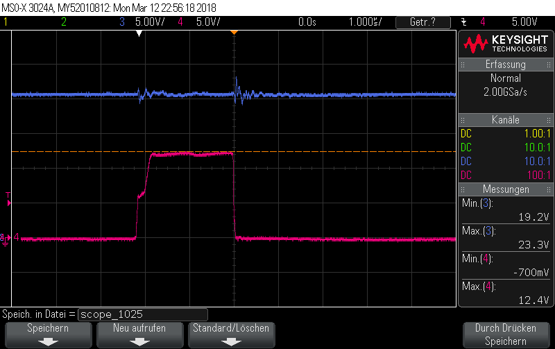
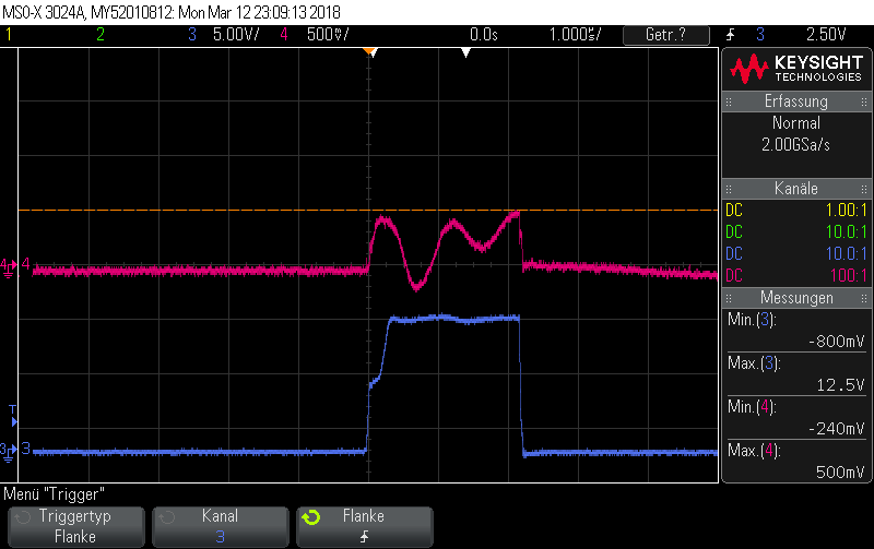
D.) DRV pin to GND_ISO (blue) and VFB (auxiliary winding) to GND_ISO (red)
E.) DRV pin to GND_ISO (blue) and voltage directly over current shunt R15 (replaced the 1.5 Ohms with 0.75 Ohms) (GND of oscilloscope connected to GND_ISO, probe with small signal to ground loop) (red)
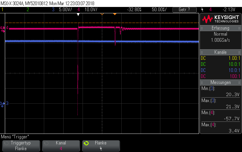
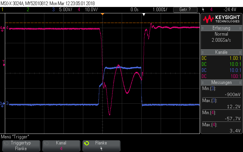
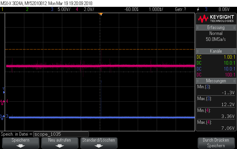
F.) DRV pin to GND_ISO (blue) and input capacitor voltage (VBAT_OUTER_FUSED_DIODE to GND_ISO) (red), zoomed red Y axis, voltage between 197.2 and 202.1 V

Discussion
It looks like the UCC28711 detects some kind of fault before sending another pulse and goes to UVLO. However, I don't see a reason for that:
Fault Protection.
- Output overvoltage fault
- Input undervoltage fault
- Internal overtemperature fault
- Primary overcurrent fault
- CS pin fault
- VS pin fault
to 1.: with the resistor divider and the waveform of the auxiliary winding, it can be calculated that the VS pin voltage is between -14.9 V and +0.88 V
to 2.: i don't understand and in fact I didn't realize that the TIDU873A is implemented with an auxiliary winding voltage below the UVLO turn-on voltage. However, the HV pin seems to be charging the input capacitor properly. I tried adding a 220 uF capacitor which significantly increased the period of the capacitor charge through the HV pin and discharge through the UCC but it didn't start as well (1 pulse). I also added the diode D9 (Figure 24 in TIDU873A) and broke the original PCB connection between C4 and C5. The period of charge/discharge was much smaller (because the effectivy capacity at the VDD pin is 1uF instead of 11 uF), so the output voltage was something around 50 V but it was still not regulated at the desired voltage of 500 V (still, 1 pulse only).
to 3.: normal lab conditions with 20-22°C, so unlikely. I don't want to touch the chip and I don't have a thermal cam in the moment but i guess the chip would fall into a longer period of idle if it was too hot.
to 4. and 5.: i tried different resistors (0.75 R, 1.5 R, 2.7 R) without success which resulted in voltages of 0.2, 0.5 and 1.0 V over the shunt and at the CS pin. Still only one pulse with all resistors. at least with 0.2 and 0.5 V it should have worked.
to 6.: I tried changing the UCC and I have two assembled versions of the PCB, so I guess a bad solder joint or something like that is not the case.
Things I tried without success:
- replaced UCC28711
- lowered R1, R2, R3, R5, R9 (connected to HV pin) to a sum of 47 kOhm
- removed the D2 (name in my schematic) zener diode
- replaced the 1K resistor R17 in parallel to D2 with 100 kOhm
- removed R6, so the LED won't be used/draw current
- checked the EN signal, which is 5V constantly
- checked the High-voltage input, which is pretty flat even during the MOSFET gate pulse
- checked the DRV signal, seems to be fine
- changed R10 (gate resistor with 1 R and 100 R)
- double-checked the pin-layout of the UCC and the transformer 750342792 (Wuerth)
I guess the Grounding is not 100% ok because there seems to be a big swing at the CS pin. However, it can't be that bad because I have a ground pane and kept the loop between the 220 nF input capacitor +/-, transformer, and MOSFET small.
The output does not draw a significant current (I think, because the output voltage sinks slowly after power-off and stays in between 22 and 28 V or close to 50 V depending on the changes I made described above. But I can measure over a shunt again next week if that should be a problem).
Does anyone have a clue what could be the fault or what exactly the chip does and why? or what i could change in my setup?
I would really appreciate your help since I have no more ideas left and I would need an insulation resistance monitor within the next weeks.
Thank you in advance and Best Regards,
Matthias Luh


