This thread has been locked.

If you have a related question, please click the "Ask a related question" button in the top right corner. The newly created question will be automatically linked to this question.

LM5161: Layout guidelines for HV pins

Part Number: LM5161

I have a customer attempting to use the LM5161.  Max operating voltage of 100V VIN will be used in the application, which creates a high voltage differential between adjacent pins (VIN/GND).

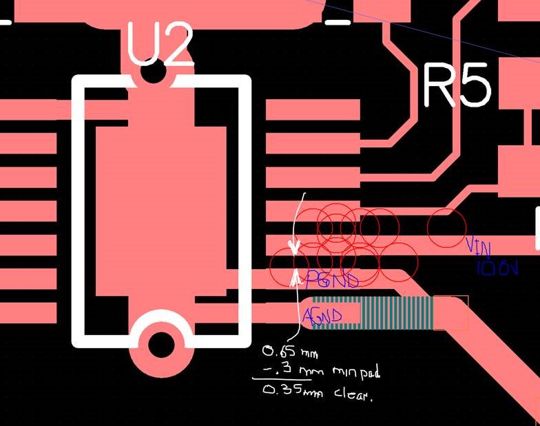
When my customer runs DRC, it is noted that clearance/creepage minimums are being violated for spacing between VIN and GND pads.

Can you provide guidance regarding how to best approach the layout for this part under max operating conditions?

  • Hello Gregory,

    The pin spacing land pattern specified in the Datasheet should be fine for 100V, the design layout rules set up in the layout Software will need to be adjusted to accommodate the land pattern pin spacing.

    Hope this helps?

    David.
  • David,

    I rechecked the creepage distance tables (for IEC60950-1 for Pollution level 2) and found that my original assumptions were incorrect.

    Those who have similar issues should check those IEC documents for their PCB DRC clearance setups.

    Sorry for the inconvenience and thanks to Greg and David, and everyone at TI.